
Method and system for testing a dual-port memory at speed in a stressed environment

a dual-port memory and stress environment technology, applied in the direction of information storage, static storage, digital storage, etc., can solve the problems of increasing the complexity involved in the testing of some memory devices, the difficulty of rapidly and cost-effectively identifying manufacturing defects of volatile memory devices, and the stress of multi-port memory cells

Active Publication Date: 2006-11-21
SYNOPSYS INC
View PDF8 Cites 43 Cited by
  • Summary
  • Abstract
  • Description
  • Claims
  • Application Information

AI Technical Summary

Problems solved by technology

Unfortunately, this trend has resulted in significantly increasing the complexity involved in the testing of some memory devices.
In particular, it has become increasingly challenging to rapidly and cost-effectively identify manufacturing defects in volatile memory devices, such as CMOS SRAM devices (i.e., complimentary metal oxide semiconductor, static random access memory devices).
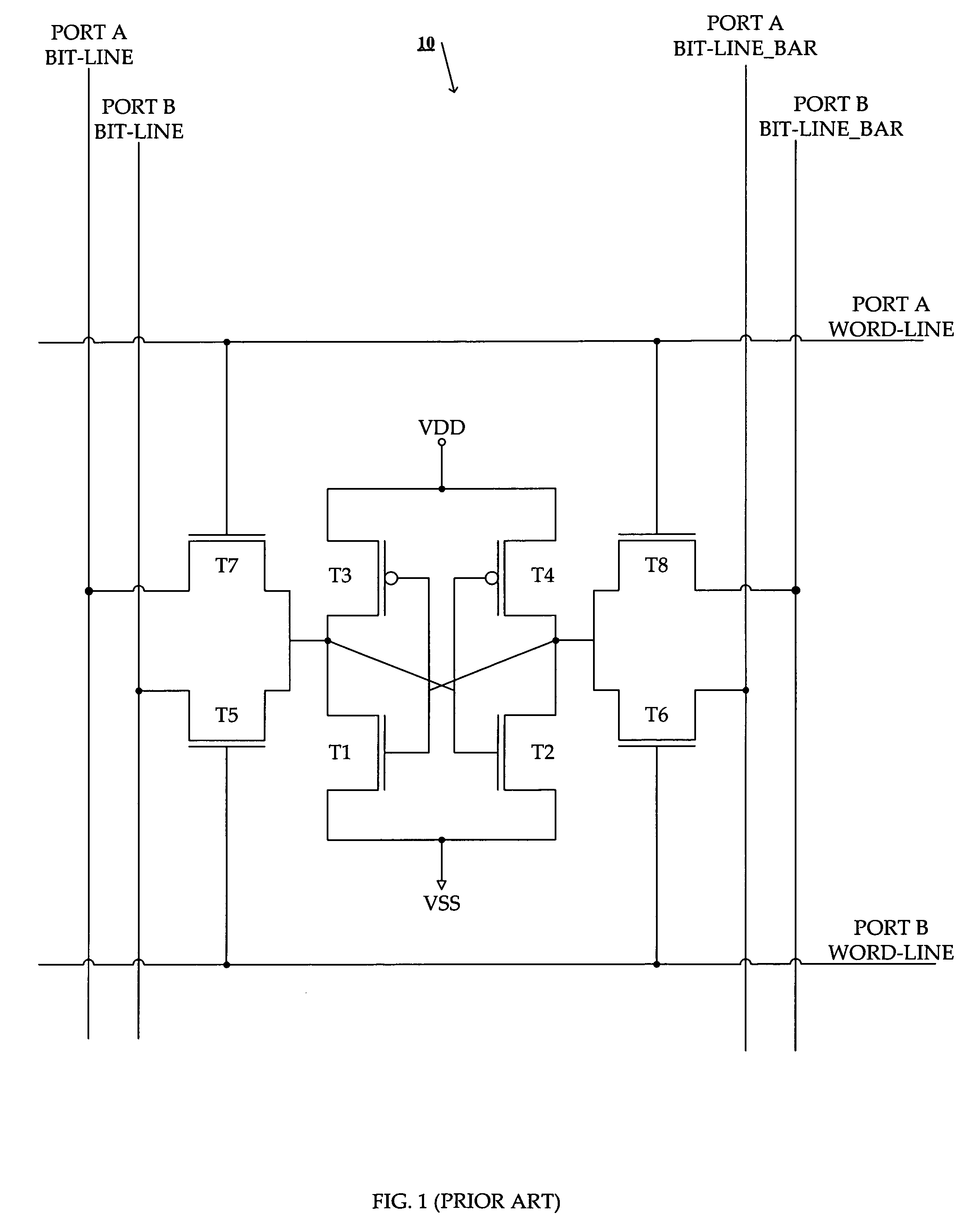
Because the storage element of the multi-port memory cell is connected to multiple ports, a multi-port memory cell may be subject to certain states and stress conditions that are difficult to emulate in a testing mode.
Consequently, traditional approaches to testing multi-port memory devices fail to test the memory cells in the stressed conditions that the memory cells may encounter during normal operation.
Another problem with traditional multi-port memory testing methods is that often the testing logic used to test the individual memory cells of the array does not operate at the clock frequency at which the device will operate under normal conditions.
Moreover, because the BISTR logic is often implemented to be physically separated from the memory core, the testing and control signals may experience a propagation delay in reaching the memory core.
Furthermore, it may take more than one clock cycle to generate and set-up the control and testing signals.
Consequently, errors that may occur when the memory device is operated at its normal operating frequency may not be detected if the memory device is tested at a frequency other than the normal operating frequency.

Method used


Image

  • Method and system for testing a dual-port memory at speed in a stressed environment
  • Method and system for testing a dual-port memory at speed in a stressed environment
  • Method and system for testing a dual-port memory at speed in a stressed environment

Examples


Embodiment Construction

[0016]In general, a method and system for testing a multi-port memory device are described. In the following description, for purposes of explanation, numerous specific details are set forth in order to provide a thorough understanding of the present invention. It will be evident, however, to one skilled in the art that the present invention may be practiced without these specific details.

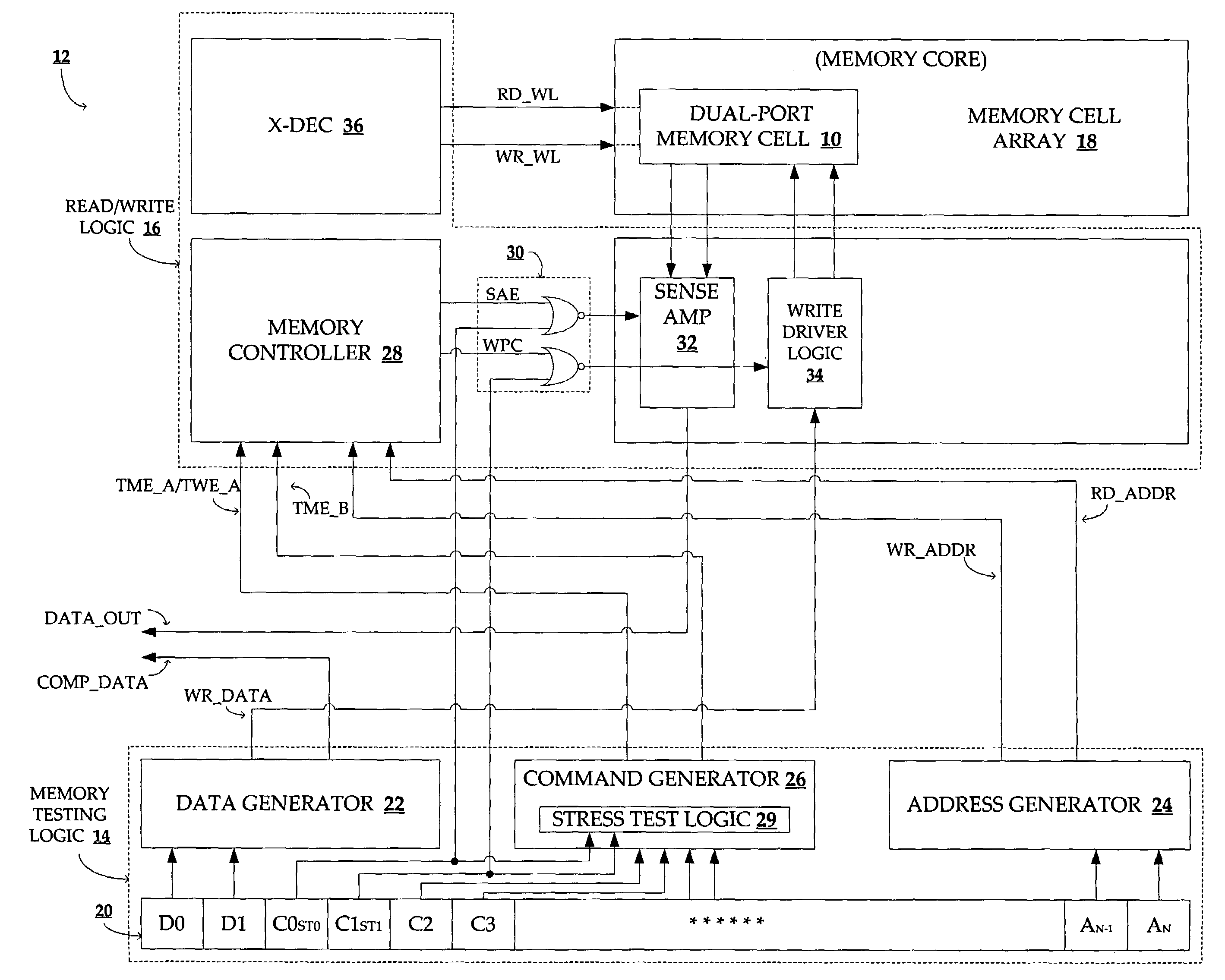
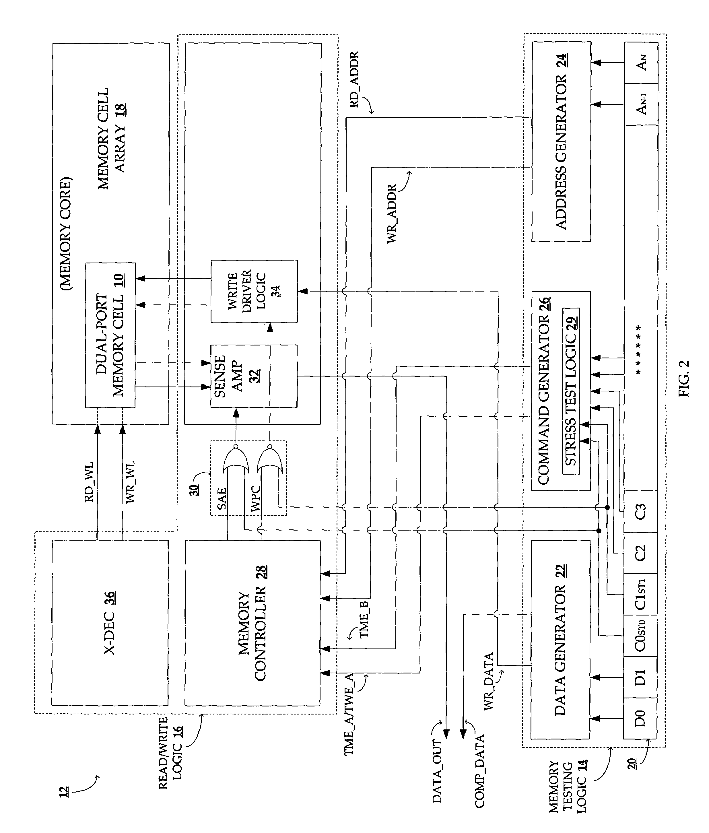
[0017]Consistent with one embodiment of the invention, a multi-port memory device includes memory testing logic that is local to the memory core and operates to test the individual multi-port memory cells of a multi-port memory cell array while the memory cells are in a stressed condition. Moreover, the individual multi-port memory cells of the memory cell array are tested at a clock frequency that is substantially equivalent to the maximum operating clock frequency of the memory device (e.g., at a frequency equivalent to the system clock). Consequently, defects in the memory cells, which may go un...


PUM


Abstract

A method and system for testing a multi-port memory cell are described. According to one embodiment of the invention, a multi-port memory device comprises an array of multi-port memory cells. Accordingly, each multi-port memory cell is connected to one word-line and two bit-lines per read / write port. The memory device includes memory testing logic to perform a first memory access operation (e.g., read / write) at a first port of the multi-port memory cell while the memory cell is in a stressed condition. For example, the first memory access operation occurs while a second memory access operation is emulated on a second port. Moreover, the memory access operations occur at a frequency that is substantially equivalent to a maximum operating frequency of the dual-port memory device.

Description

RELATED APPLICATIONS[0001]The present application is related to and claims the benefit of the filing date of U.S. Provisional Patent Application with Ser. No. 60 / 577,897, filed on Jun. 7, 2004, which is hereby incorporated herein by reference.TECHNICAL FIELD[0002]The present invention relates generally to the testing of solid-state memory devices. More particularly, the present invention relates to an improved method and system for testing dual-port memory cells at speed in a stressed condition.BACKGROUND[0003]As fabrication methods have improved and smaller geometry technologies, such as 90-nanometer design, have been developed, the area of silicon required to produce a memory device having a given data storage capacity has continued to decrease. Generally, these technological advances have led to a greater number of memory devices per silicon wafer, and consequently, a lower cost per memory device. Meanwhile, the overall storage capacity of memory devices has been continuously inc...

Claims


Application Information

Patent Timeline
IPC IPC(8): G11C29/00
CPCG11C29/16G11C8/16G11C2029/3602
Inventor BEHERA, NIRANJAN
Owner SYNOPSYS INC
Learn More