Electronic package for image sensor, and the packaging method thereof

a technology of image sensor and electronic packaging, which is applied in the direction of semiconductor devices, semiconductor/solid-state device details, radiation control devices, etc., can solve the problems of insufficient size of the package, and inability to meet the requirements of hand-held applications such as cellular phones, and achieves a simple and convenient use. , the effect of high cost-effective sealing techniqu

Active Publication Date: 2006-11-28
OPTOPAC
View PDF22 Cites 76 Cited by
  • Summary
  • Abstract
  • Description
  • Claims
  • Application Information

AI Technical Summary

Benefits of technology

[0030]Accordingly, it is an object of the present invention to provide a simple and conveniently employed, and highly cost-effective sealing technique for image sensor packaging.

Problems solved by technology

Therefore, such plastic package is generally not suitable as electronic packaging for image sensors.
However, it is ordinarily very expensive.
Moreover, the package in most cases is not small enough for hand-held applications like cellular phones.
However, it is not as robust as the ceramic package, and is no more compact than a comparable ceramic package.
This option may prove a bit cheaper in cost, but also fails to provide the degree of compactness normally required for hand-held applications.
The packages mentioned above fail to provide sufficient compactness for hand-held applications such as cellular phone.
This special requirement limits the package's application in practice.
However, there are several critical drawbacks in this technique.
The most critical drawback is that the structure is too complicated, and the process technique is too difficult.
Because of these drawbacks, required manufacturing costs tend to be prohibitively high, and sufficiently high yields tend to be difficult to achieve, which in turn also increases overall manufacturing costs.
Other drawbacks are found with this technique.
This results in additional costs.
Yet another disadvantage to this technique is that all dice on wafers are subjected to all the manufacturing processes in this technique.
The manufacturing cost depends quite heavily on the yield of each image sensor wafer in this kind of situation.
Given such circumstances, it is not easy to adopt this technique for packaging an image sensor wafer.
A major source of failure in image sensor packaging is particles adhered to image sensing area surfaces.
This causes repeatable spotting in the resultant digital images.
Even though particles may not actually stick to image sensing area surfaces, but instead moves inside of the package, the persistent if not repeatable spotting which results in the resultant digital images is equally unacceptable.
Contamination of the image sensing area otherwise may cause the same kind of failure.
First of all, this package requires a vacuum solder reflow process instead of a conventional convection reflow process or the like.
As the solder material melts and wets to pads on the substrate, the solder sealing ring necessarily tends toward some collapse.
This would increase failure rate in forming solder joints, which in turn increases yield loss.
Residual solvent in the cavity would prove detrimental to long term reliability, and may also cause contamination of the image sensing area.
A vacuum reflow technique, on the other hand, is not common in industry even though it has been tried for research purposes.
Hence, there is no vacuum reflow equipment for mass production commercially available presently on the market.
The temperature control would not be as simple as for a conventional belt oven.
The required fluxless soldering for forming this package structure would add further costs and complexity.

Method used


Image

  • Electronic package for image sensor, and the packaging method thereof
  • Electronic package for image sensor, and the packaging method thereof
  • Electronic package for image sensor, and the packaging method thereof

Examples


Embodiment Construction

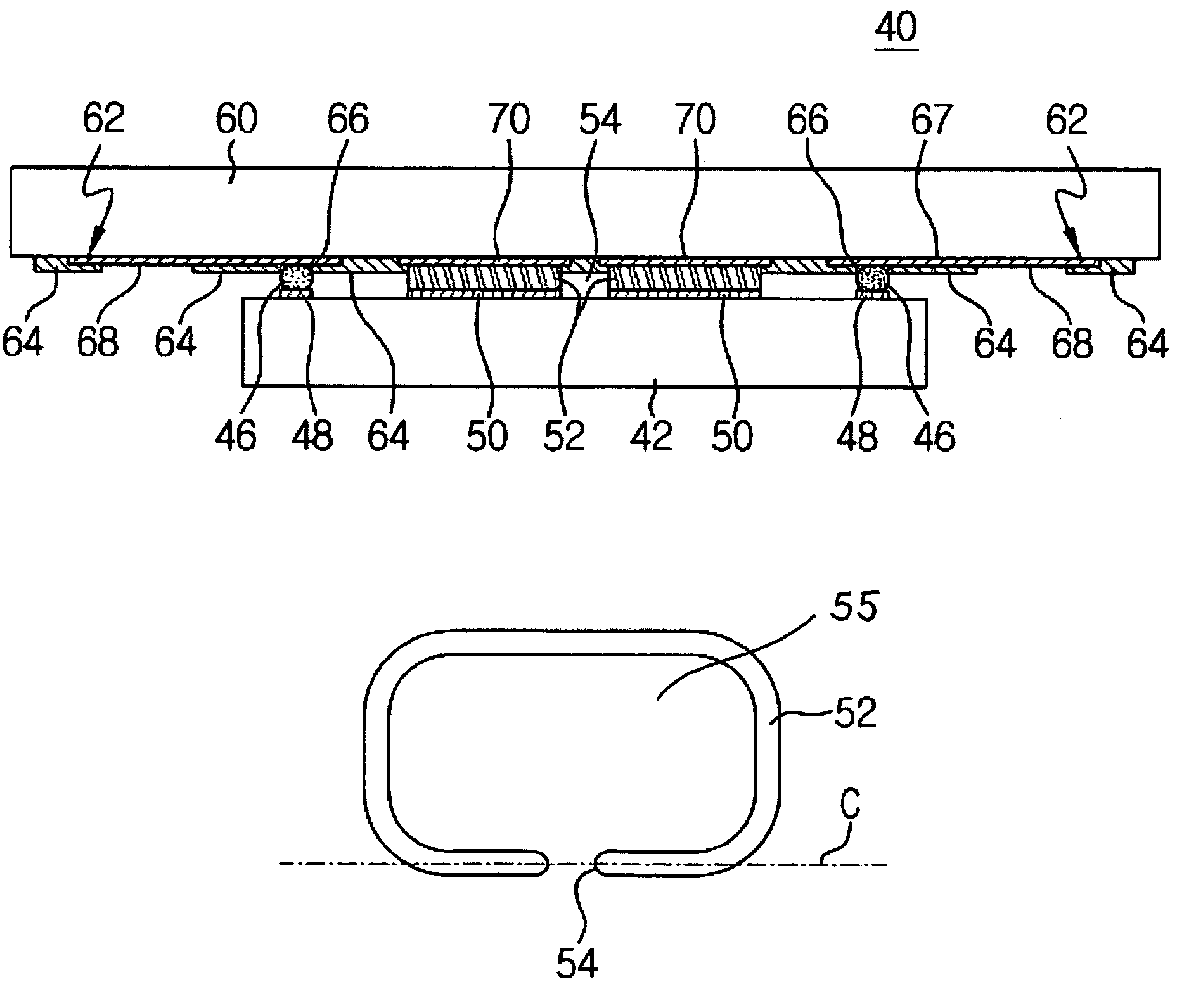
[0070]An electronic package 40 formed in accordance with one exemplary embodiment of the present invention, is schematically illustrated in FIGS. 5a and 5b. The package 40 includes an image sensor die 42, which is formed with at least one image sensing area 44. The image sensor die 42 includes electrical terminals, preferably in the form of so called “bonding pads” about a peripheral area thereof. The image sensor die 42 further includes solder bump pads 48 that are electrically connected to the bonding pads. The image sensor die 42 also includes a solder sealing ring pad(s) 50 formed substantially about the image sensing area.

[0071]The electronic package 40 of the present invention, as shown in FIGS. 5a and 5b, additionally includes a substrate 60. The substrate 60 is formed of a material having substantial transparency in the range of wavelengths of light that the image sensor detects. The substrate is provided with at least one patterned metal layer 62 and at least one patterned ...


PUM


Abstract

A semiconductor device package and method for its fabrication are provided. The semiconductor device package generally includes at least one semiconductor die and a substrate coupled to the semiconductor die. The semiconductor die is provided with a front side defining a sealing area, and a first solder sealing ring pad formed on that front side. The substrate is provided with a front surface opposing the front side of the semiconductor die on which a second solder sealing ring pad is formed. A solder sealing ring structure is sandwiched between the first and second solder sealing pads of the substrate and semiconductor die, such that it extends peripherally about a substantial portion of the sealing area to substantially enclose thereat a cavity between the semiconductor die and the substrate. The solder sealing ring structure includes at least one venting portion defining against at least one of the substrate and semiconductor die an air vent in open communication with the cavity.

Description

RELATED APPLICATION DATA[0001]This Application is based on Korean Patent Application, Ser. No. 10-2004-0090584, filed 8 Nov. 2004.BACKGROUND OF THE INVENTION[0002]1. Field of the Invention[0003]The present invention relates generally to electronic packaging of semiconductor integrated circuits. More specifically, the present invention relates to electronic packaging of image-sensing semiconductor devices.[0004]2. Related Art[0005]Image sensors (or image-sensing semiconductor devices) find wide use in various digital photography applications. They are used in digital cameras and camcorder, for which the market has grown sharply since about 1999 when manufacturers began incorporating in cellular phone devices.[0006]As shown in FIG. 1, an image sensor die 2 includes an image-sensing area 4 (the so-called “pixel area”) at its center, and electrical terminals 6 (the so-called “bonding pads”) about its peripheral areas for electrical input and output. Typically, the image-sensing area 4 i...

Claims


Application Information

Patent Timeline
Patent Type & Authority Patents(United States)
IPC IPC(8): H01L23/495H01L27/14H01L23/02H01L27/146H01L31/0203
CPCH01L27/14618H01L31/0203H01L2224/29011H01L2224/48091H01L2224/48227H01L2924/01077H01L2924/01078H01L2924/01079H01L2924/09701H01L2924/16195H01L2924/1461H01L2924/01322H01L2224/45144H01L2224/73203H01L2924/00014H01L2924/00H01L2924/00012H01L23/02H01L27/14
Inventor KIM, DEOK-HOONLEE, HWAN-CHUL
Owner OPTOPAC
Why Eureka
Try Eureka