Circuit for controlling an enabling time of an internal control signal according to an operating frequency of a memory device and the method thereof

a technology of internal control signal and operating frequency, which is applied in the direction of information storage, static storage, digital storage, etc., can solve the problems of high cost and time, and the inability to correct the variation of the pulse width of the read/write strobe pulse, so as to reduce the pulse width of the signal outpu

Active Publication Date: 2006-11-28
SK HYNIX INC
View PDF15 Cites 13 Cited by
  • Summary
  • Abstract
  • Description
  • Claims
  • Application Information

AI Technical Summary

Benefits of technology

[0021]According to another aspect of the present invention, there is also provided a method of delaying a signal outputted from a read / write strobe pulse generator by applying an external address signal and controlling a width of the read / write pulse.
[0025]In this embodiment, as a cycle period of the clock signal is shorter, a pulse width of the first signal is narrower.
[0029]In this embodiment, it further comprises the step of (b-2) more reducing a pulse width of a signal outputted from the step (d) by using an address signal of the memory device.

Problems solved by technology

In a conventional art, while the delay time of the delay circuit 20 is variable by modifying a metal option during a FIB process when an operating frequency of the memory device varies, it needs much costs and times.
In addition, with the conventional art, there is no way to correct a variation of the pulse width of the read / write strobe pulse signal rdwtstbzp13 when an operation voltage of the memory device varies.

Method used


Image

  • Circuit for controlling an enabling time of an internal control signal according to an operating frequency of a memory device and the method thereof
  • Circuit for controlling an enabling time of an internal control signal according to an operating frequency of a memory device and the method thereof
  • Circuit for controlling an enabling time of an internal control signal according to an operating frequency of a memory device and the method thereof

Examples


Embodiment Construction

[0042]Reference will now be made in greater detail to a preferred embodiment of the invention, an example of which is illustrated in the accompanying drawings. Wherever possible, the same reference numerals will be used throughout the drawings and the description to refer to the same or like parts.

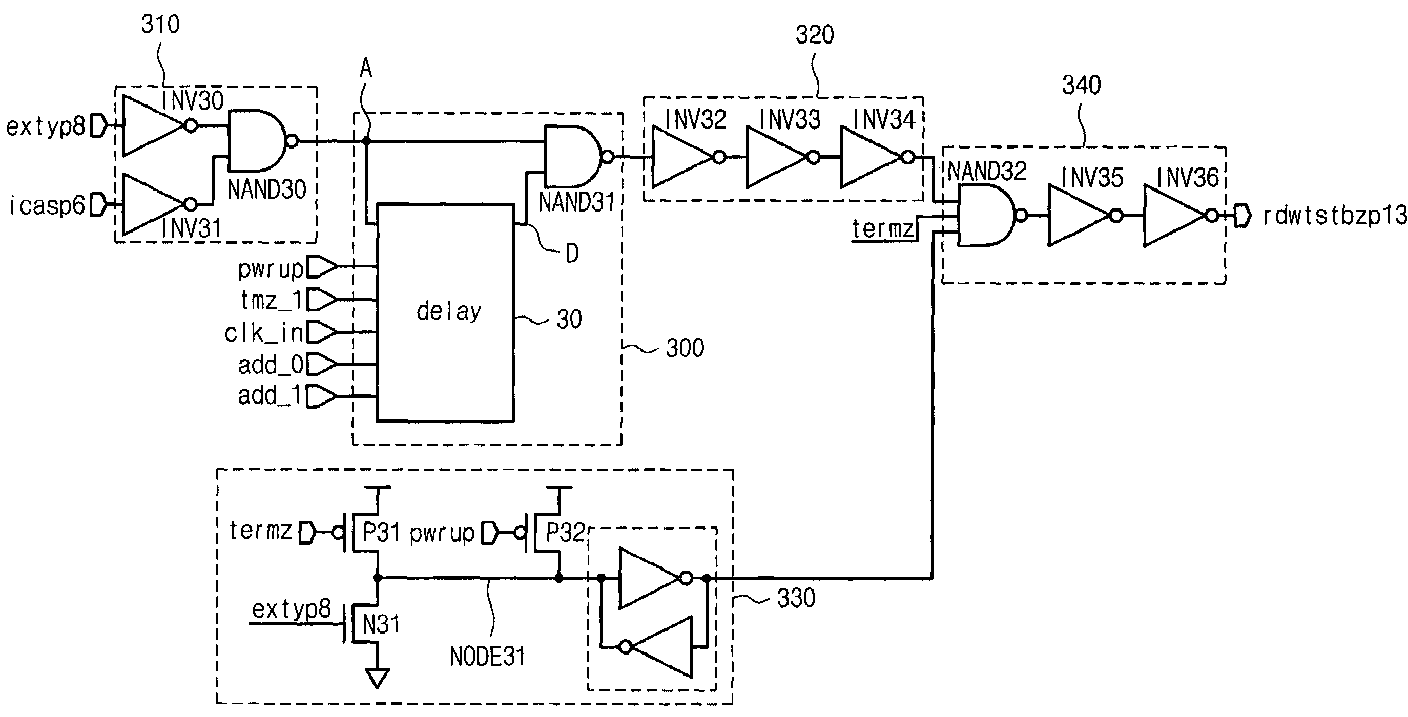
[0043]FIG. 3 illustrates an exemplary embodiment of a read / write strobe pulse generator in accordance with the present invention.

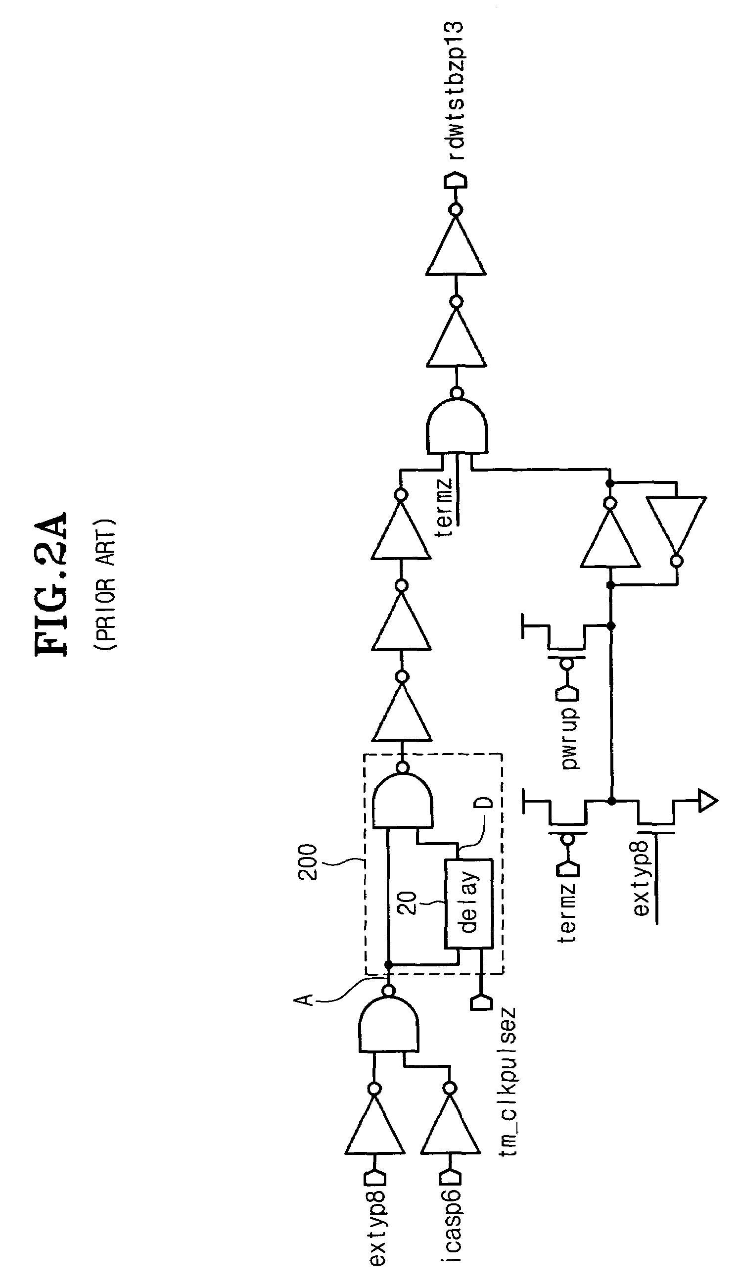
[0044]The circuit of FIG. 3 is different from the circuit of FIG. 2A in that a delay circuit 30 in a pulse width adjusting circuit 300 is controlled by a clock signal clk_in and address signals add_0 and add_1.

[0045]The circuit of FIG. 3 is comprised of an input signal receiver 310, a pulse width adjusting circuit 300, a signal transmission circuit 320, a test mode circuit 330, and an output circuit 340.

[0046]The input signal receiver 310 includes inverters INV30 and INV31, and a NAND gate NAND30. An input signal extyp8 is applied to the inverter INV30 and an inp...


PUM


Abstract

Provided is a circuit for controlling a data bus connecting a bitline sense amplifier to a data sense amplifier in accordance with a variation of an operating frequency of a memory device, being comprised of a pulse width adjusting circuit for varying a pulse width of an input signal in accordance with the operating frequency of the memory device after receiving the input signal, a signal transmission circuit for buffing a signal outputted from the pulse width adjusting circuit, and an output circuit for outputting a first signal to control the data bus in response to a signal outputted from the signal transmission circuit.

Description

BACKGROUND OF THE INVENTION[0001]1. Field of the Invention[0002]The present invention relates to a method for controlling a sense amplifier of a memory device, and more particularly, to a method and circuit for automatically controlling an operation of a sense amplifier in correspondence with variations of operating voltage and frequency of a memory device.[0003]2. Description of the Related Art[0004]FIG. 1 is a diagram illustrating a read and write operations in a general memory device.[0005]As shown in FIG. 1, during a write operation, data applied through an input / output data pad is transferred to a bitline sense amplifier through a data input buffer and a data input register. While, during a read operation, cell data amplified by the bitline sense amplifier is transferred to the input / output data pad through a data sense amplifier, a pipe register, and a data output buffer.[0006]In FIG. 1, signal Yi is a pulse signal to connect the bitline sense amplifier with the data sense amp...

Claims


Application Information

Patent Timeline
Patent Type & Authority Patents(United States)
IPC IPC(8): G11C7/00G11C7/08G11C7/06G11C7/10G11C29/02
CPCG11C7/1048G11C29/50012G11C29/028G11C29/02G11C7/06
Inventor KIM, JI HYUNNAM, YOUNG JUN
Owner SK HYNIX INC
Why Eureka
Try Eureka