Creating optimized physical implementations from high-level descriptions of electronic design using placement-based information

a technology of placement-based information and high-level descriptions, applied in the direction of cad circuit design, program control, instruments, etc., can solve the problems of inability to produce efficient physical implementations of many circuit designs by top-down design methodologies, and designers using conventional top-down eda tools struggle with the creation, analysis and verification of integrated circuits., and achieve the effects of improving density, power, and productivity

Inactive Publication Date: 2006-11-28
SYNOPSYS INC
View PDF19 Cites 78 Cited by
  • Summary
  • Abstract
  • Description
  • Claims
  • Application Information

AI Technical Summary

Benefits of technology

[0016]The present invention overcomes the limitations of the conventional top-down methodology with an RTL optimization system and method that enhances existing top-down EDA systems by implementing an automatic performance-driven design paradigm. The RTL optimization system of the present invention implements automatic hierarchical structured custom design and delivers significant improvements in performance, density, power, and productivity over the existing top-down design methodology. The RTL design methodology of the present invention enables the user to enter, analyze, debug, optimize, and implement their designs by working exclusively with RTL models before logic synthesis. Full-chip design, analysis, and optimization run orders-of-magnitude faster than conventional gate-level tools, thereby enabling truly interactive design.

Problems solved by technology

Each of these flows involve multiple time consuming iterations, and the exchange of very complex information.
While the synthesis and place-and-route automation represent a significant productivity improvement over an otherwise tedious and error-prone manual design process, the top-down design methodology has failed to produce efficient physical implementations of many circuit designs that take full advantage of the capability of advanced IC manufacturing processes.
In contrast, designers using conventional top-down EDA tools struggle with the creation, analysis, and verification of integrated circuits having 0.5–1 million gates, running at 150 MHz.
The primary inefficiency of the top-down methodology arises from its reliance on statistical wire-load models proved to be inadequate in wire-delay dominated deep sub-micron digital systems.
These tools use inaccurate, statistical wire-load estimates to model wiring parasitics at early stages in the design cycle, and the effects of these inaccuracies are propagated throughout the rest of the design methodology.
The large discrepancy between statistical wire-load model and actual wire-load means that circuit designers must wait until gate-level floorplanning and place and route tasks are complete to begin chip-level optimization.
The enormous gate-level complexity of today's system-on-a-chip designs places a heavy burden on gate-level verification and analysis tools and makes multiple design iterations very time consuming.
Additionally, the complexity of present high performance integrated circuit designs overwhelms the capability of logic synthesis tools.
Place-and-route execution times for these circuits can also consume many hours.
Thus, logic synthesis cannot process complex designs all at once.
During manual partitioning, however, the designer has little or no accurate information on the back-end physical effect of the partitioning, and in particular, on the effect of such partitions on timing, area, and power consumption.
The failure to predict accurate back-end physical effect at or above the RTL design stage results in local optimization and a sub-optimal functional description of the design.
Design efficiency suffers due to design over-constraint (timing non-convergence) or under-constraint (loss of performance and density), or some combination of both for various different partitions of the integrated circuit.
Sub-optimal RTL descriptions and partitioning serve as a poor starting point for logic synthesis, which propagates and amplifies the design deficiencies, eventually leading to silicon inefficiency (e.g., excessive area or power consumption, slower operating frequency), even after long iteration and manual intervention.
Further inefficiency in the top-down design methodology is introduced because logic synthesis tools treat all logic as random logic.
Consequently, logic synthesis typically fails to recognize and take advantage of more efficient silicon structures such as datapaths, which are commonly used and expressed in the high level description of the design.
This is equivalent to writing a gate-level netlist, an onerous, low-productivity, and error-prone task.
Another deficiency of the top-down methodology is that it requires a cumbersome netlist hand-off between front-end and back-end design cycles.
The diverse design expertise required to effectively manage the top-down design process is rare and not commonly available to a typical design team.
Design inefficiency causes the costly under-utilization of advanced IC manufacturing processes.
The iterative nature of the top-down design methodology requires long design time and large design teams, often not available or even feasible in a competitive design environment characterized by short product life-cycles and short time-to-market requirements.
Thus, achieving rapid timing convergence while satisfying density, power, and productivity constraints for high performance complex systems is a daunting challenge facing the electronic design industry today.

Method used


Image

  • Creating optimized physical implementations from high-level descriptions of electronic design using placement-based information
  • Creating optimized physical implementations from high-level descriptions of electronic design using placement-based information
  • Creating optimized physical implementations from high-level descriptions of electronic design using placement-based information

Examples


Embodiment Construction

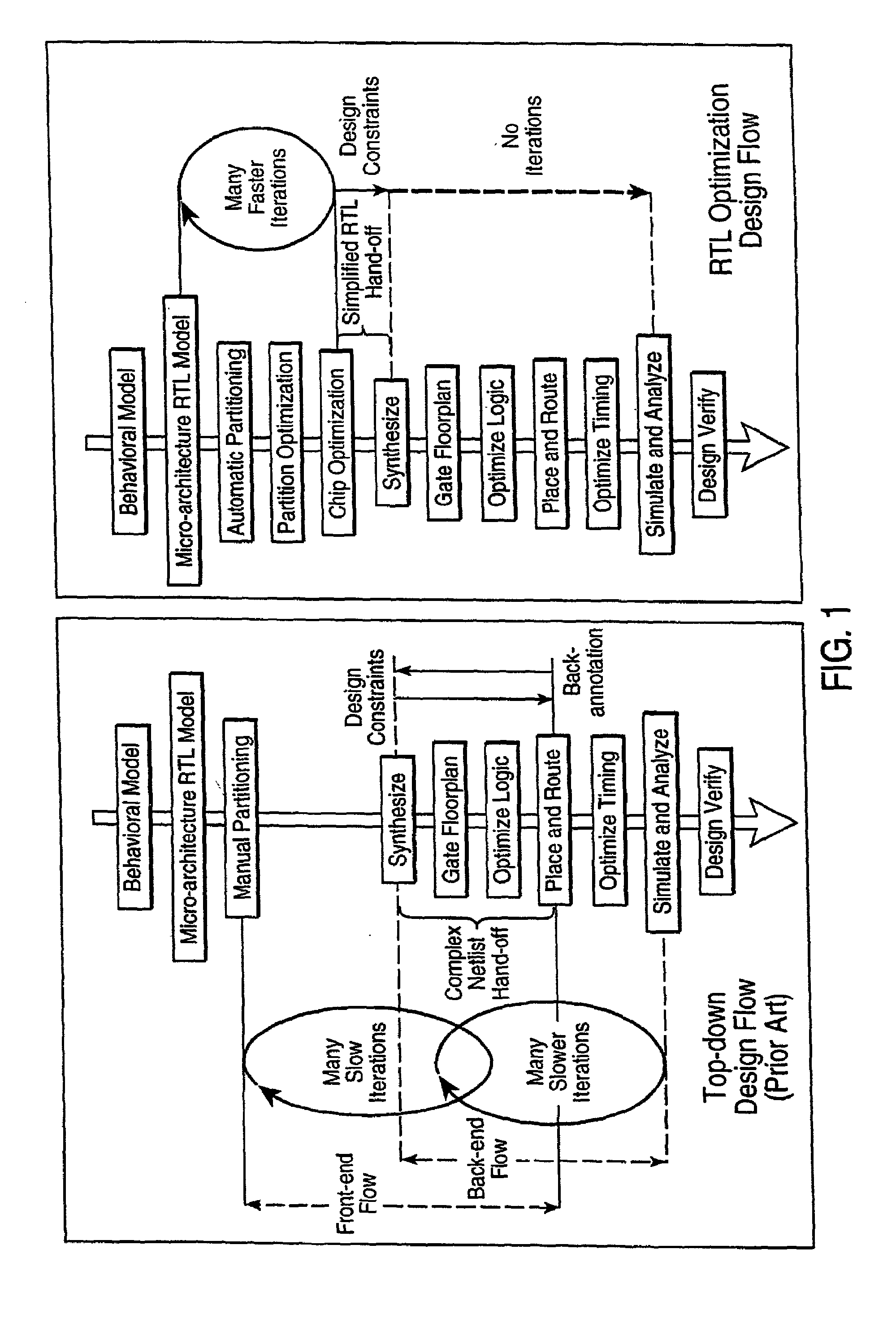
1. Overview of the RTL Optimization Process

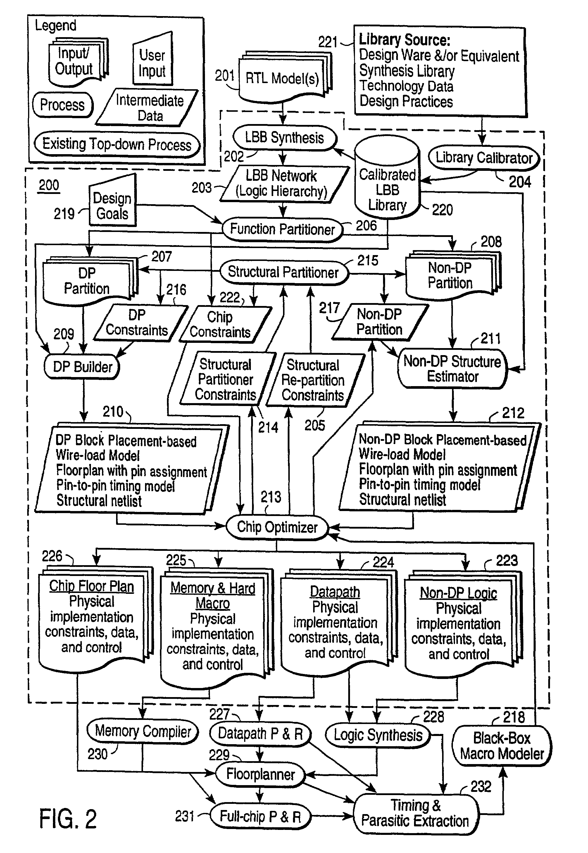
[0053]Referring now to FIG. 2 there is shown a data-flow diagram of a RTL optimization system 200 for optimizing an electronic design in accordance with the present invention. The RTL optimization system 200 is designed to converge automatically on the best solution for an electronic design that satisfies the design goals. At the end of the automatic processes provided by the system 200, manual intervention for the purpose of design refinement is allowed.

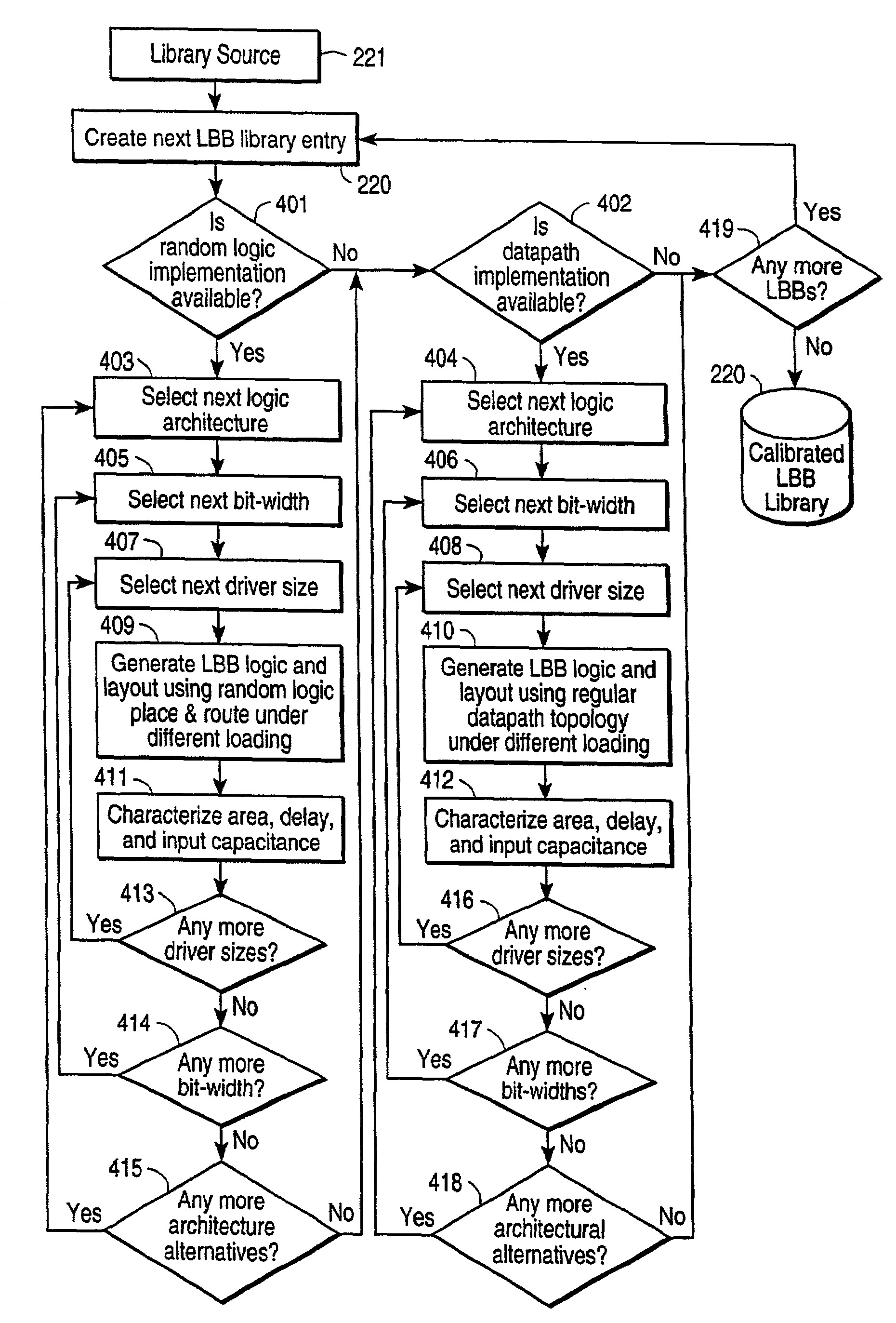
[0054]The following steps are employed in the RTL optimization system 200:[0055]Synthesize 202 the RTL model to a LBB network[0056]Enter chip-level design goals 219[0057]Functional partitioning 206[0058]Feasible block-level implementation 209&211[0059]Chip optimization 213[0060]Structural partitioning 215[0061]Chip re-optimization 213 (2nd pass)

[0062]The system 200 operates on a conventional computer system, such as an Intel based personal computer using the Microsoft Corp.'s Windows NT ope...


PUM


Abstract

An electronic design automation system provides optimization of RTL models of electronic designs, to produce detailed constraints and data precisely defining the requirements for the back-end flows leading to design fabrication. The system takes a RTL model of an electronic design and maps it into an efficient, high level hierarchical representation of the hardware implementation of the design. Automatic partitioning partitions the hardware representation into functional partitions, and creates a fully characterized performance envelope for a range of feasible implementations for each of the partitions, using accurate placement based wire load models. Chip-level optimization selects and refines physical implementations of the partitions to produce compacted, globally routed floorplans. Chip-level optimization iteratively invokes re-partitioning passes to refine the partitions and to recompute the feasible implementations. In this fashion, a multiple-pass process converges on an optimal selection of physical implementations for all partitions for the entire chip that meet minimum timing requirements and other design goals. The system outputs specific control and data files which thoroughly define the implementation details of the design through the entire back-end flow process, thereby guaranteeing that the fabricated design meets all design goals without costly and time consuming design iterations.

Description

CROSS REFERENCE TO RELATED APPLICATIONS[0001]This application is a continuation of U.S. patent application Ser. No. 09 / 634,927, filed Aug. 8, 2000 U.S. Pat. No. 6,360,356, which is a continuation of U.S. patent application Ser. No. 09 / 015,602, filed Jan. 30, 1998, now U.S. Pat. No. 6,145,117.BACKGROUND OF THE INVENTION[0002]1. Field of the Invention[0003]The present invention relates generally to methods and systems used to create efficient physical implementations from high level descriptions of electronic designs and, in particular, to a software system and method that optimizes Register-Transfer-Level (RTL) descriptions with respect to performance parameters including area, timing, and power, prior to logic synthesis, floorplanning, placement and routing.[0004]2. Description of the Background Art[0005]Present Electronic Design Automation (EDA) systems for designing electronic systems consist of software tools running on a digital computer that assist a designer in the creation an...

Claims


Application Information

Patent Timeline
Patent Type & Authority Patents(United States)
IPC IPC(8): G06F17/50
CPCG06F17/5045G06F17/5068G06F17/5072G06F2217/78G06F2217/84G06F30/39G06F30/30G06F30/392G06F2119/12G06F2119/06G06F30/3947
Inventor ENG, TOMMY K
Owner SYNOPSYS INC
Why Eureka
Try Eureka