Creating optimized physical implementations from high-level descriptions of electronic design using placement-based information

Inactive Publication Date: 2006-03-09
MAGMA DESIGN AUTOMATION
View PDF14 Cites 71 Cited by
  • Summary
  • Abstract
  • Description
  • Claims
  • Application Information

AI Technical Summary

Benefits of technology

[0016] The present invention overcomes the limitations of the conventional top-down methodology with an RTL optimization system and method that enhances existing top-down EDA systems by implementing an automatic performance-driven design paradigm. The RTL optimization system of the present invention implements automatic hierarchical structured custom design and delivers significant improvements in performance, density,

Problems solved by technology

Each of these flows involve multiple time consuming iterations, and the exchange of very complex information.
While the synthesis and place-and-route automation represent a significant productivity improvement over an otherwise tedious and error-prone manual design process, the top-down design methodology has failed to produce efficient physical implementations of many circuit designs that take full advantage of the capability of advanced IC manufacturing processes.
In contrast, designers using conventional top-down EDA tools struggle with the creation, analysis, and verification of integrated circuits having 0.5-1 million gates, running at 150 MHz.
The primary inefficiency of the top-down methodology arises from its reliance on statistical wire-load models proved to be inadequate in wire-delay dominated deep sub-micron digital systems.
These tools use inaccurate, statistical wire-load estimates to model wiring parasitics at early stages in the design cycle, and the effects of these inaccuracies are propagated throughout the rest of the design methodology.
The large discrepancy between statistical wire-load model and actual wire-load means that circuit designers must wait until gate-level floorplanning and place and route tasks are complete to begin chip-level optimization.
The enormous gate-level complexity of today's system-on-a-chip designs places a heavy burden on gate-level verification and analysis tools and makes multiple design iterations very time consuming.
Additionally, the complexity of present high performance integrated circuit designs overwhelms the capability of logic synthesis tools.
Place-and-route execution times for these circuits can also consume many hours.
Thus, logic synthesis cannot process complex designs all at once.
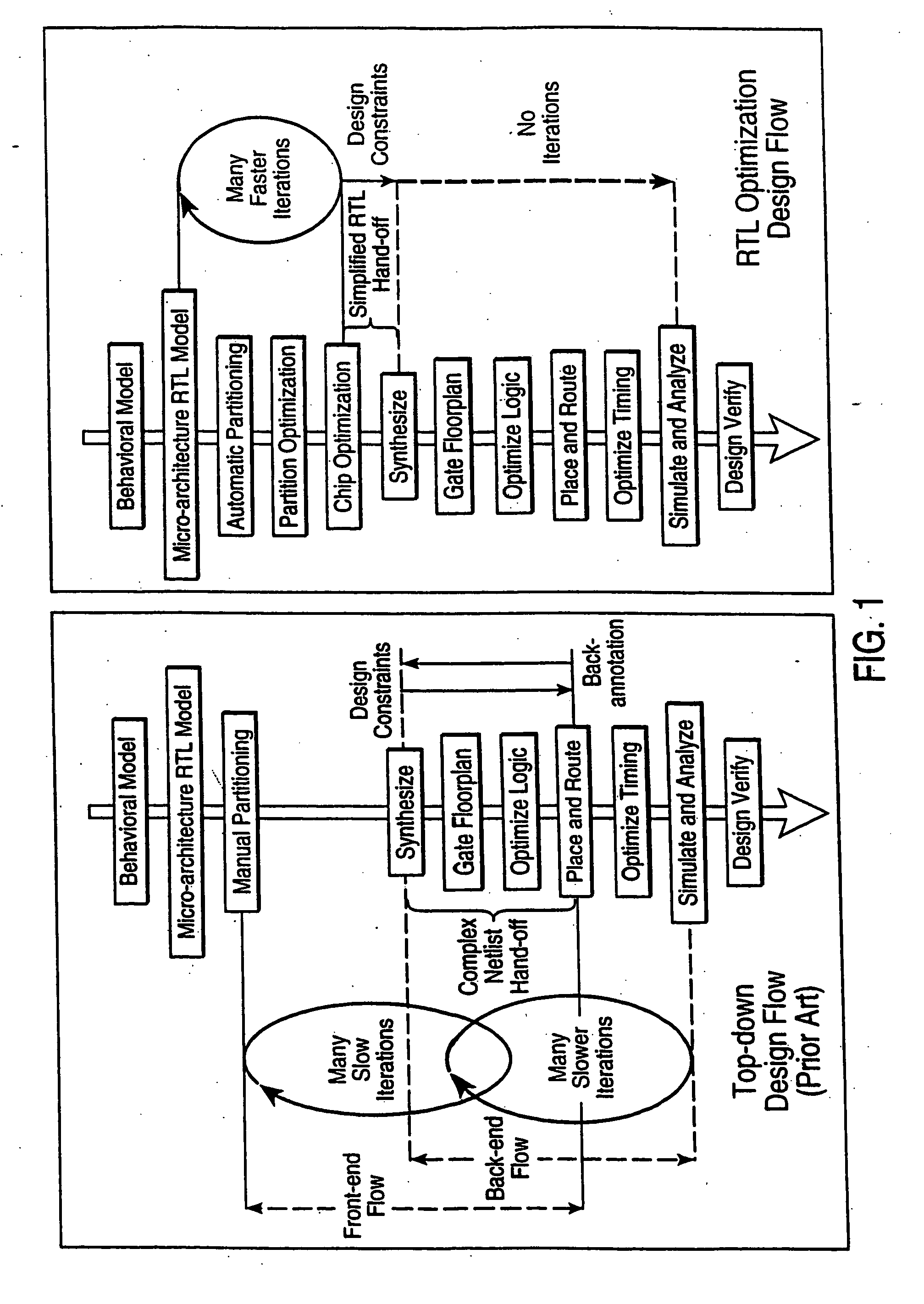
During manual partitioning, however, the designer has little or no accurate information on the back-end physical effect of the partitioning, and in particular, on the effect of such partitions on timing, area, and power consumption.
The failure t

Method used


Image

  • Creating optimized physical implementations from high-level descriptions of electronic design using placement-based information
  • Creating optimized physical implementations from high-level descriptions of electronic design using placement-based information
  • Creating optimized physical implementations from high-level descriptions of electronic design using placement-based information

Examples


Embodiment Construction

1. Overview of the RTL Optimization Process

[0053] Referring now to FIG. 2 there is shown a data-flow diagram of a RTL optimization system 200 for optimizing an electronic design in accordance with the present invention. The RTL optimization system 200 is designed to converge automatically on the best solution for an electronic design that satisfies the design goals. At the end of the automatic processes provided by the system 200, manual intervention for the purpose of design refinement is allowed.

[0054] The following steps are employed in the RTL optimization system 200: [0055] Synthesize 202 the RTL model to a LBB network [0056] Enter chip-level design goals 219[0057] Functional partitioning 206[0058] Feasible block-level implementation 209&211[0059] Chip optimization 213[0060] Structural partitioning 215[0061] Chip re-optimization 213 (2nd pass)

[0062] The system 200 operates on a conventional computer system, such as an Intel based personal computer using the Microsoft Corp.'...


PUM


Abstract

An electronic design automation system provides optimization of RTL models of electronic designs, to produce detailed constraints and data precisely defining the requirements for the back-end flows leading to design fabrication. The system takes a RTL model of an electronic design and maps it into an efficient, high level hierarchical representation of the hardware implementation of the design. Automatic partitioning partitions the hardware representation into functional partitions, and creates a fully characterized performance envelope for a range of feasible implementations for each of the partitions, using accurate placement based wire load models. Chip-level optimization selects and refines physical implementations of the partitions to produce compacted, globally routed floorplans. Chip-level optimization iteratively invokes re-partitioning passes to refine the partitions and to recompute the feasible implementations. In this fashion, a multiple-pass process converges on an optimal selection of physical implementations for all partitions for the entire chip that meet minimum timing requirements and other design goals. The system outputs specific control and data files which thoroughly define the implementation details of the design through the entire back-end flow process, thereby guaranteeing that the fabricated design meets all design goals without costly and time consuming design iterations.

Description

CROSS REFERENCE TO RELATED APPLICATIONS [0001] This application is a continuation of U.S. patent application Ser. No. 09 / 634,927, filed Aug. 8, 2000, which is a continuation of U.S. patent application Ser. No. 09 / 015,602, filed Jan. 30, 1998, now U.S. Pat. No. 6,145,117.BACKGROUND OF THE INVENTION [0002] 1. Field of the Invention [0003] The present invention relates generally to methods and systems used to create efficient physical implementations from high level descriptions of electronic designs and, in particular, to a software system and method that optimizes Register-Transfer-Level (RTL) descriptions with respect to performance parameters including area, timing, and power, prior to logic synthesis, floorplanning, placement and routing. [0004] 2. Description of the Background Art [0005] Present Electronic Design Automation (EDA) systems for designing electronic systems consist of software tools running on a digital computer that assist a designer in the creation and verification...

Claims


Application Information

Patent Timeline
IPC IPC(8): G06F17/50G06F9/45
CPCG06F17/5045G06F17/5068G06F2217/84G06F2217/78G06F17/5072G06F30/39G06F30/30G06F30/392G06F2119/12G06F2119/06G06F30/3947
Inventor ENG, TOMMY K.
Owner MAGMA DESIGN AUTOMATION
Why Eureka
Try Eureka