
Upgrade of optical amplifier site to a digital optical network site in an optical transmission network

a technology of optical transmission network and optical amplifier, applied in the field of optical transmission network, can solve problems such as not being aware of digital signals

Active Publication Date: 2006-12-12
INFINERA CORP
View PDF20 Cites 19 Cited by
  • Summary
  • Abstract
  • Description
  • Claims
  • Application Information

AI Technical Summary

Benefits of technology

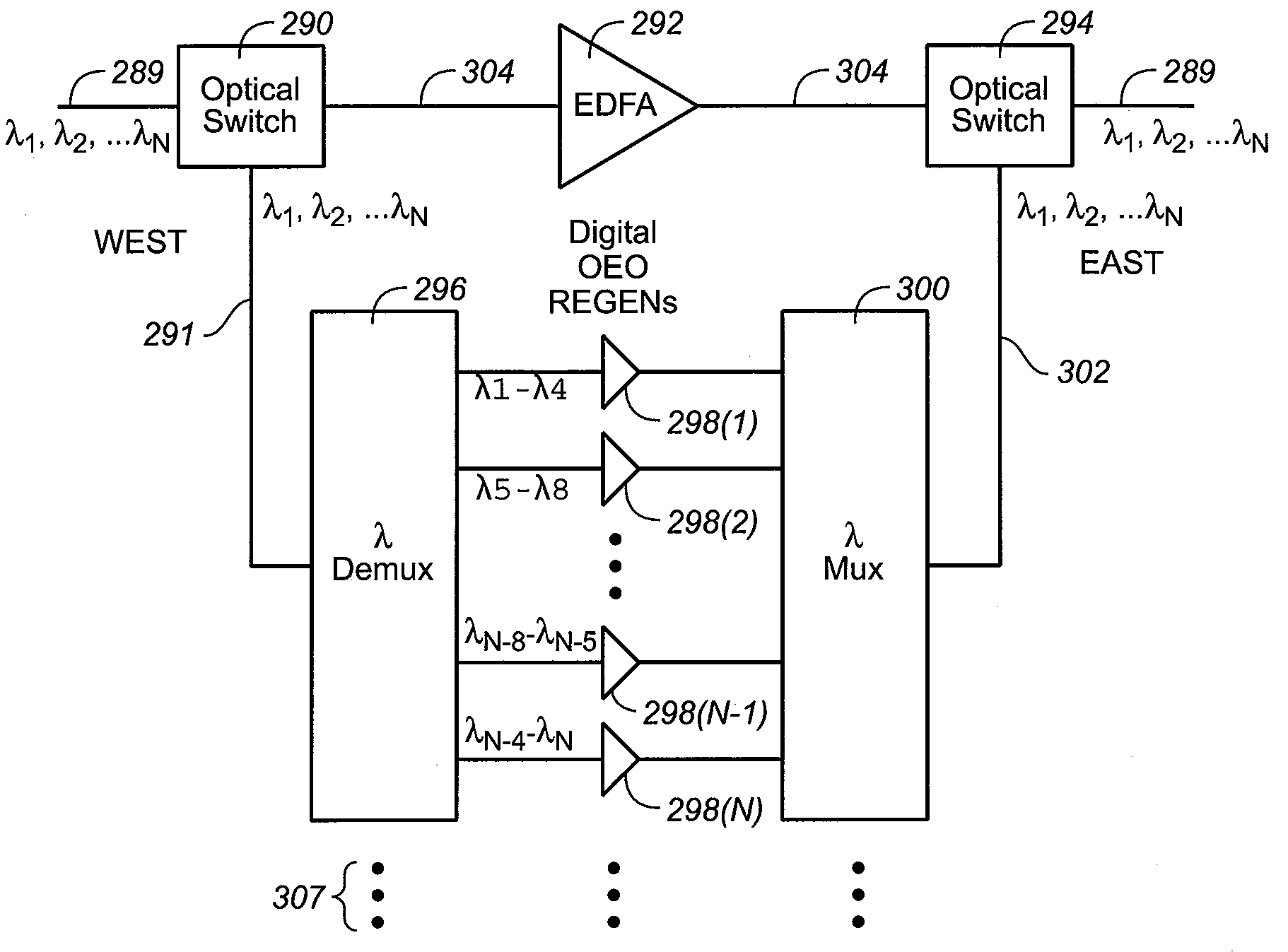
[0093]According to this invention, a digital signal channel bypass is provided as bypass around an optical network optical amplifier, in particular, an analog type optical amplifier, such as an EDFA, in an optical transport network or system. The digital signal bypass provides for an ability to maintain the existing optical amplifier OO amplification site while inserting a bypass that provides ultra low-cost OEO REGEN in a digital optical network (DON) utilizing both semiconductor electronic integrated circuit chips and semiconductor photonic integrated circuit (PIC) chips where all the optical components are in semiconductor integrated chip form providing 1R, 2R, 3R or 4R regeneration as well as other signal caring functionality. A salient feature of the digital signal bypass is to regenerate signals in the optical span that are outside the gain bandwidth of the EDFA or other such amplifier.

Problems solved by technology

However, we are not aware of any digital signal OEO bypass as set forth herein for 3R bypass of an OFA, such as an EDFA site deployed in an optical span of an optical transport network.

Method used


Image

  • Upgrade of optical amplifier site to a digital optical network site in an optical transmission network
  • Upgrade of optical amplifier site to a digital optical network site in an optical transmission network
  • Upgrade of optical amplifier site to a digital optical network site in an optical transmission network

Examples


first embodiment

[0151]In the digital optical bypass of this invention, which is illustrated in FIGS. 21–24, the bypassing channels may be dropped, groomed, backhauled, amplified or wavelength translated or converted as required. such a digital optical bypass in one directional network, such as for East-bound channel traffic, is illustrated in FIG. 21. Along the optical span 289 on either side of EDFA 292 and its coupling fibers 304 there are provided in-line optical switches 290 and 294. These optical switches have switching speeds on the order of 1 to 10 msec and are deployed to move channel traffic around EDFA 292, such as through an OEO REGEN 104 or junction site 106 (FIG. 8), A / D site 114 (FIG. 9) or site 178 (FIG. 17). Switching on this scale, although not totally absent of loss, can be successful in certain types of customer installations especially in the case of IP routers. Microsecond optical switches are available but at higher cost.

[0152]As shown in FIG. 21, all the signal channels, λ1, ...

second embodiment

[0159]The second embodiment in FIG. 22 is the same as that shown in FIG. 21 except that EDFA 293 provides for bidirectional digital signal regeneration on optical fiber link 289 so that all or some of the channel traffic, whether east bond signal channels, λi . . . λN, or west bound signal channels, λj . . . λM, can be diverted, via optical switch 290 or 294, respectively, through the optical bypass via line 291 or 302, respectively, to mux / demux 297 or 301, respectively, and the individual signal channels, λi . . . λN or λj . . . λM, respectively, provided with 3R functioning or ADD / DROP multiplexing, grooming, switching or routing functioning via respective digital OEO REGENs 299(1), 299(2). . . 299(N-1), 299(N). Thus, the principal of the embodiment of FIG. 22 is bidirectional in the sense that west bound traffic can be treated through the digital bypass in the same manner as the East bound traffic performing signal caring functions as outline above and in connection with the emb...

third embodiment

[0160]Reference is now made to a third embodiment shown in FIG. 23 which is illustrates a unidirectional digital OEO REGEN bypass comprising this invention similar to FIG. 21 except, in the case here, signal channel bands, λB1, λB2, etc. are selectively bypassed at first stage band demultiplexer 303 and re-multiplexed at first stage band multiplexer 316. As in the case of FIG. 21, the embodiment of FIG. 23 may be a bidirectional signal regeneration system as illustrated in FIG. 22. In FIG. 23, first stage band demux 303 filters or demultiplexes the channel wavelength bands, λB1 and λB2, for example, so that channel band, λB1 (signal channels, for example, λI . . . λn), is directed via bypass optical line 306 to a second stage demux 308 while channel band, λB2 (signal channels, for example, λJ . . . λm), is directed via coupling fiber 304 for amplification via EDFA 292. At second stage band demux 308, the signal channels, λI . . . λn, of channel band, λB1, are demultiplexed into indi...


PUM


Abstract

A digital signal channel bypass is provided as bypass around an optical network optical amplifier, in particular, an analog type optical amplifier, such as an EDFA, in an optical transport network or system. The digital signal bypass provides for an ability to maintain the existing optical amplifier OO amplification site while inserting a bypass that provides ultra low-cost OEO REGEN in a digital optical network (DON) utilizing both semiconductor electronic integrated circuit chips and semiconductor photonic integrated circuit (PIC) chips where all the optical components are in semiconductor integrated chip form providing 1R, 2R, 3R or 4R regeneration as well as other signal caring functionality. A salient feature of the digital signal bypass is to regenerate signals in the optical span that are outside the gain bandwidth of the EDFA or other such amplifier.

Description

CROSS REFERENCE TO RELATED APPLICATIONS[0001]This application claims priority to provisional application Ser. No. 60 / 392,494 filed Jun. 28, 2002 and entitled, DIGITAL OPTICAL NETWORK ARCHITECTURE, now nonprovisional application Ser. No. 10 / 267,212, filed Oct. 8, 2002, also published on May 29, 2003 as Pub. No. US 2003 / 0099018 A1; which applications are incorporated herein by their reference.BACKGROUND OF THE INVENTION[0002]1. Field of the Invention[0003]This invention relates generally to optical transport networks and more particularly to an upgrade of analog optical amplifier sites or nodes in optical transport networks through the deployment of a bypass analog amplifier site or node with a digital amplifier site or node comprising low cost, compact optical-electrical-optical (OEO) regeneration (REGEN) module.[0004]2. Description of the Related Art[0005]If used throughout this description and the drawings, the following short terms have the following meanings unless otherwise stat...

Claims


Application Information

Patent Timeline
IPC IPC(8): H04B10/00H01S3/00
CPCH04B10/291H04B10/2939H04J14/02H04J14/0221H04B2210/258H04J14/0206H04J14/0208H04J14/0209H04J14/0213
Inventor GRUBB, STEPHEN G.MITCHELL, MATTHEW L.TAYLOR, ROBERT B.DOMINIC, VINCENT G.NILSSON, ALAN C.
Owner INFINERA CORP
Learn More