
Memory cell with plasma-grown oxide spacer for reduced DIBL and Vss resistance and increased reliability

a memory cell and oxide spacer technology, applied in the field of memory device fabrication, can solve the problems of short channel effect known as drain induced barrier lowering (dibl) can undesirably increase, detrimentally affect memory cell performance, and undesirably reduce effective channel length, so as to reduce dibl and vss resistance, reduce dibl, and increase reliability

Active Publication Date: 2006-12-19
MONTEREY RES LLC
View PDF4 Cites 7 Cited by
  • Summary
  • Abstract
  • Description
  • Claims
  • Application Information

AI Technical Summary

Benefits of technology

"The present invention is about a memory cell with a plasma-grown oxide spacer that reduces resistance and increases reliability. The invention addresses the need for a floating gate flash memory cell with reduced resistance. The method includes forming a first spacer, a high energy implant doped region, and a recess in the source region of the substrate. A second spacer is then formed to connect to the source. The second spacer helps reduce drain induced barrier lowering (DIBL) in the memory cell. The technical effect of the invention is to improve the performance and reliability of the memory cell."

Problems solved by technology

However, by introducing the amount and depth of doping required to sufficiently lower Vss resistance, the effective channel length can be undesirably reduced.
As a result, a short channel effect known as drain induced barrier lowering (DIBL) can undesirably increase in a flash memory cell, such as a floating gate flash memory cell.
As a result of DIBL, the memory cell's threshold voltage decreases, which detrimentally affects memory cell performance.

Method used


Image

  • Memory cell with plasma-grown oxide spacer for reduced DIBL and Vss resistance and increased reliability
  • Memory cell with plasma-grown oxide spacer for reduced DIBL and Vss resistance and increased reliability
  • Memory cell with plasma-grown oxide spacer for reduced DIBL and Vss resistance and increased reliability

Examples


Embodiment Construction

[0018]The present invention is directed to a memory cell with plasma-grown oxide spacer for reduced DIBL and Vss resistance and increased reliability. The following description contains specific information pertaining to the implementation of the present invention. One skilled in the art will recognize that the present invention may be implemented in a manner different from that specifically discussed in the present application. Moreover, some of the specific details of the invention are not discussed in order not to obscure the invention.

[0019]The drawings in the present application and their accompanying detailed description are directed to merely exemplary embodiments of the invention. To maintain brevity, other embodiments of the present invention are not specifically described in the present application and are not specifically illustrated by the present drawings.

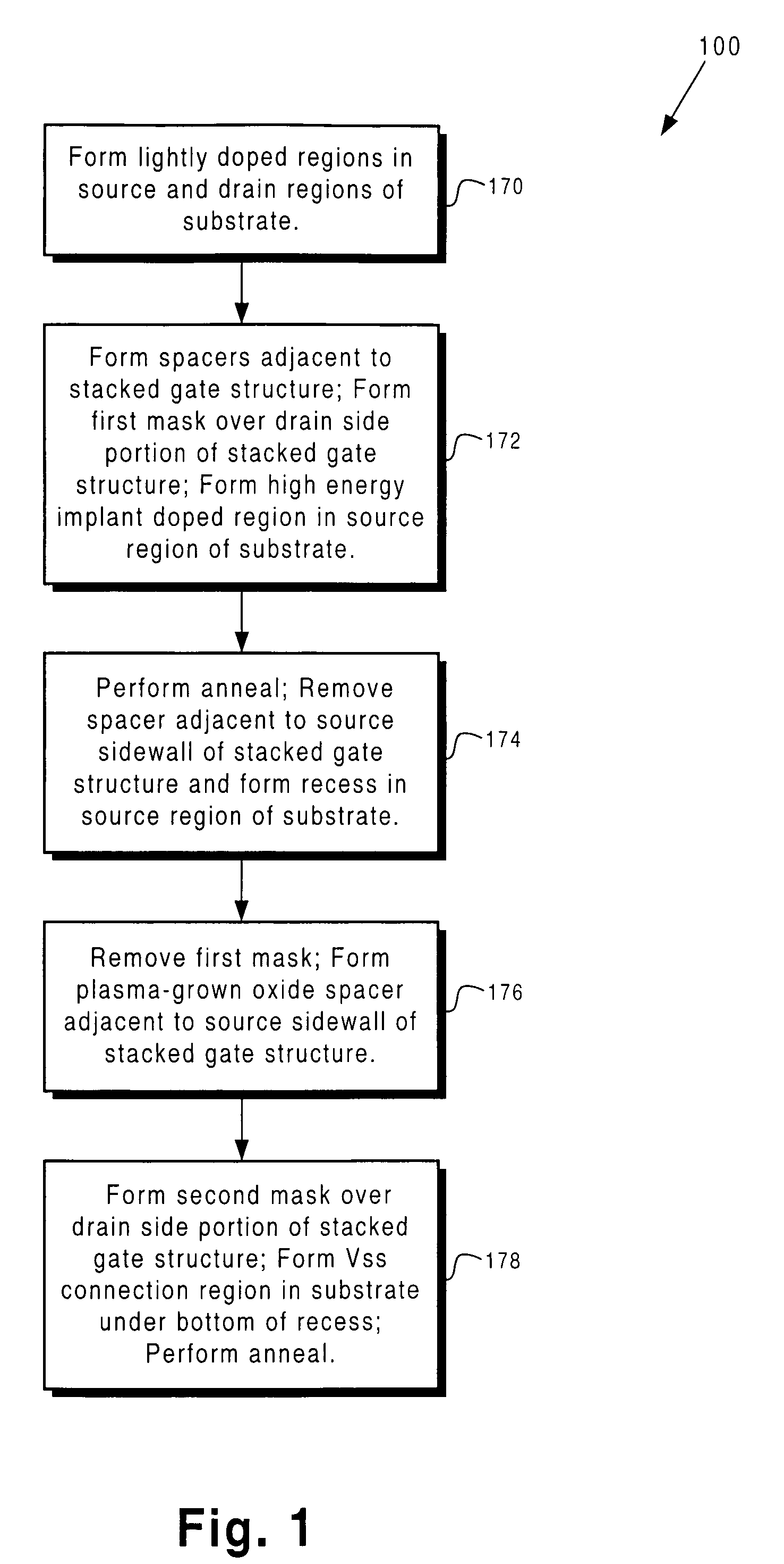
[0020]FIG. 1 shows a flowchart illustrating an exemplary method for forming a floating gate flash memory cell includ...


PUM


Abstract

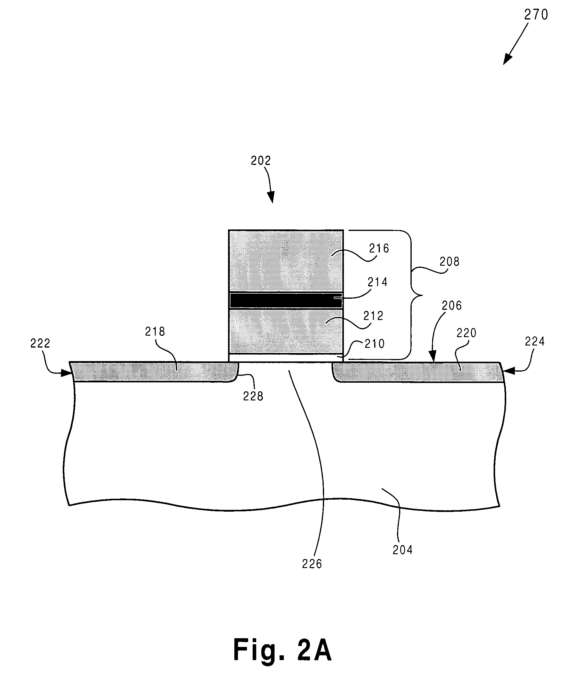
According to one exemplary embodiment, a method for fabricating a floating gate memory cell on a substrate comprises a step of forming a first spacer adjacent to a source sidewall of a stacked gate structure, where the stacked gate structure is situated over a channel region in the substrate. The method further comprises forming a high energy implant doped region adjacent to the first spacer in a source region of the substrate. The method further comprises forming a recess in the source region, where a sidewall of the recess is situated adjacent to a source of the floating gate memory cell, and where forming the recess comprises removing the first spacer. The method further comprises forming a second spacer adjacent to the source sidewall of the stacked gate structure, where the second spacer extends to a bottom of the recess, and where the second spacer comprises plasma-grown oxide.

Description

TECHNICAL FIELD[0001]The present invention is generally in the field of semiconductor fabrication. More particularly, the present invention is in the field of memory device fabrication.BACKGROUND ART[0002]High performance flash memory devices, such as NOR-type flash memory devices, require high density and high operating speed as the device dimensions are scaled down. A low resistance Vss line, which connects source regions of flash memory cells situated between word lines, is used to reduce memory core cell size, improve circuit density, and increase flash memory device performance.[0003]In a conventional flash memory process flow, the Vss line can be formed by heavily doping the semiconductor substrate by using a Vss connection implant. In order to achieve a desirably low Vss resistance, a sufficient amount and a sufficient depth of doping are required along the Vss line in the semiconductor substrate. However, by introducing the amount and depth of doping required to sufficiently...

Claims


Application Information

Patent Timeline
Patent Type & Authority Patents(United States)
IPC IPC(8): H01L21/26
CPCH01L29/1037H01L29/66636H01L29/66659H01L29/66825H01L29/7881
Inventor FANG, SHENQINGSUGINO, RINJICHANG, KUO-TUNGWANG, ZHIGANGMIZUTANI, KAZUHIROFASTENKO, PAVEL
Owner MONTEREY RES LLC
Learn More