Multiple-gate MOSFET device with lithography independent silicon body thickness and methods for fabricating the same

a mosfet transistor and lithography independent technology, applied in the field of semiconductor devices, can solve the problems of increasing off-state current, limiting the extent to which transistor dimensions can be reliably scaled, and performance limitations are also a barrier to scaling conventional planar transistor dimensions, so as to reduce the effect of short channel effects, avoiding or reducing adverse effects

Inactive Publication Date: 2005-09-20
TEXAS INSTR INC
View PDF10 Cites 61 Cited by
  • Summary
  • Abstract
  • Description
  • Claims
  • Application Information

AI Technical Summary

Benefits of technology

[0009]The invention relates to triple-gate and other multi-gate MOS transistors and methods for fabricating such transistors, in which the transistors are constructed from a semiconductor body formed above a starting structure using a form structure or mold and spacers, rather than by etching into an SOI wafer. This allows control over channel dimensions independent of lithography limitations and avoidance or mitigation of the adverse effects of etched channel surfaces, while attaining the advantages of multi-gate devices (e.g., inversion of more channel silicon, reduction in short channel effects, reduced DIBL, etc.), using less expensive starting structures (e.g., silicon wafers, etc.). In addition, the spacers may be formed (e.g., L-shaped) so as to create an undercut or re-entrant cavity at the bottom of the formed semiconductor body. The gate structure can be formed to extend within the undercut recess, thus providing for quadruple-gate or 3.5-gate transistors having semiconductor bodies smaller than a lithographically patterned gate length dimension. In one example, a form structure is provided over a semiconductor wafer with an opening exposing a portion of the wafer. A spacer is formed along sidewalls of the opening and semiconductor material is deposited in the opening by epitaxial growth, and the form structure and the spacer are then removed. A gate structure is thereafter formed along the top and sides of a central portion of the formed semiconductor body. The spacer may be L-shaped, providing an undercut or recess at the bottom of the semiconductor body sidewall, and the gate may extend into the undercut area to underlie a portion of the resulting transistor channel.

Problems solved by technology

However, lithography generally limits the extent to which transistor dimensions can be reliably scaled, wherein the minimum gate length is typically limited to the smallest dimension that can be reliably and repeatably patterned and etched using current photolithographic and etching techniques.
In addition to fabrication process limitations, performance limitations are also a barrier to scaling conventional planar transistor dimensions, particularly the gate length.
In shorter channel devices, however, the channel region is also affected by the source and drain voltages, leading to increased off-state current due to Vt roll off, degraded subthreshold slope, and degraded output current.
In practice, however, the conventional multi-gate approaches have suffered from cost and performance shortcomings, because SOI wafers are more expensive than ordinary silicon substrates and because the channel surface has been etched while carving the upper SOI silicon layer into islands or blocks.

Method used


Image

  • Multiple-gate MOSFET device with lithography independent silicon body thickness and methods for fabricating the same
  • Multiple-gate MOSFET device with lithography independent silicon body thickness and methods for fabricating the same
  • Multiple-gate MOSFET device with lithography independent silicon body thickness and methods for fabricating the same

Examples


Embodiment Construction

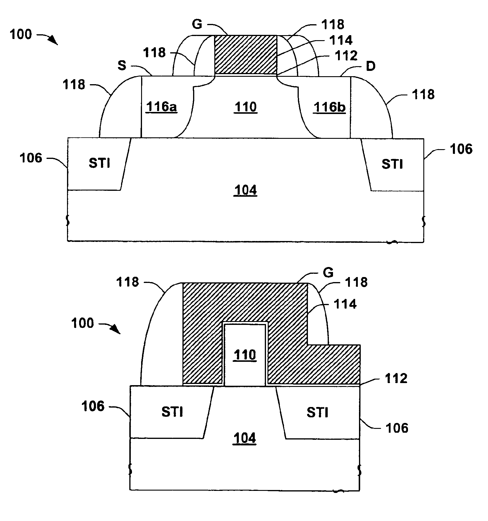
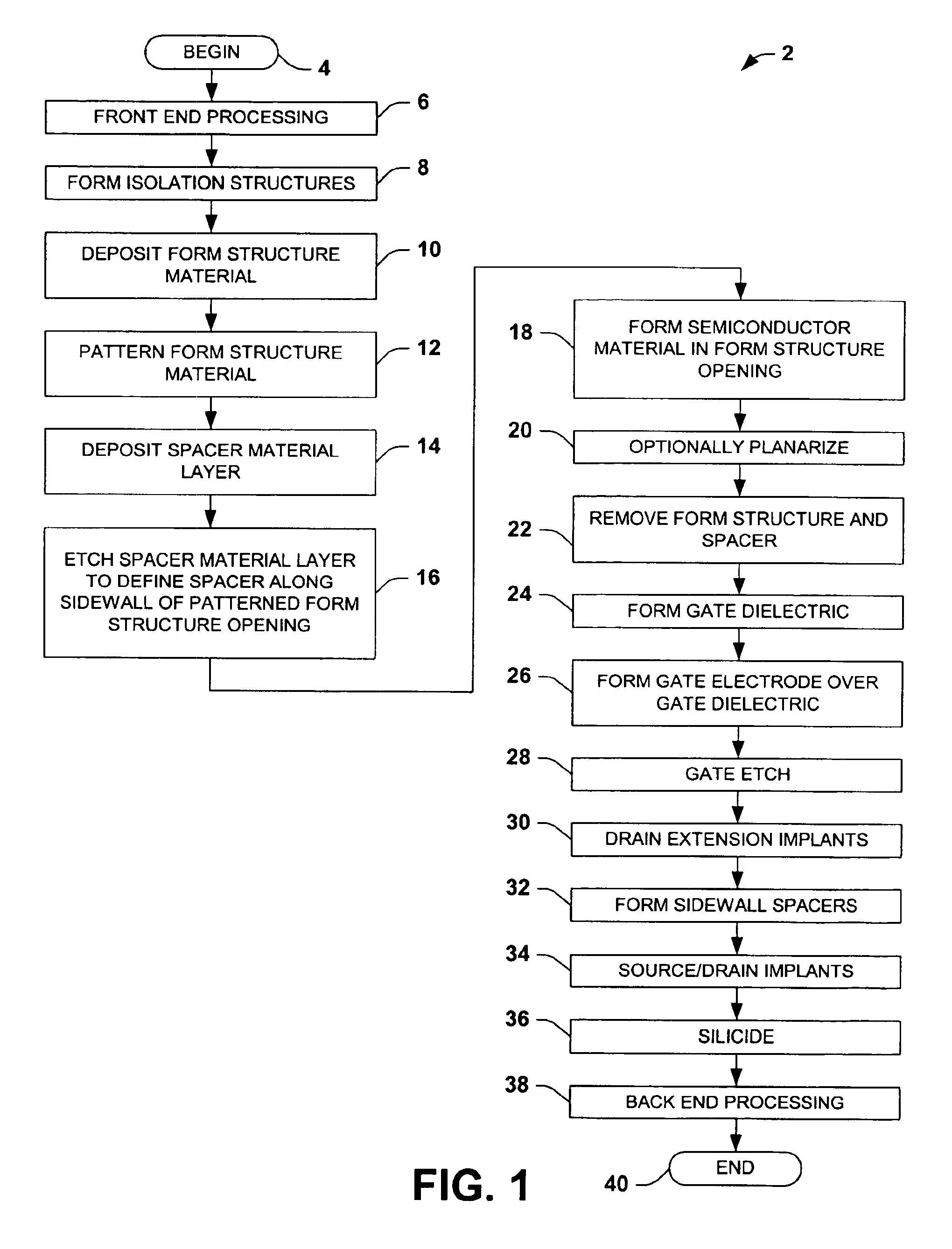
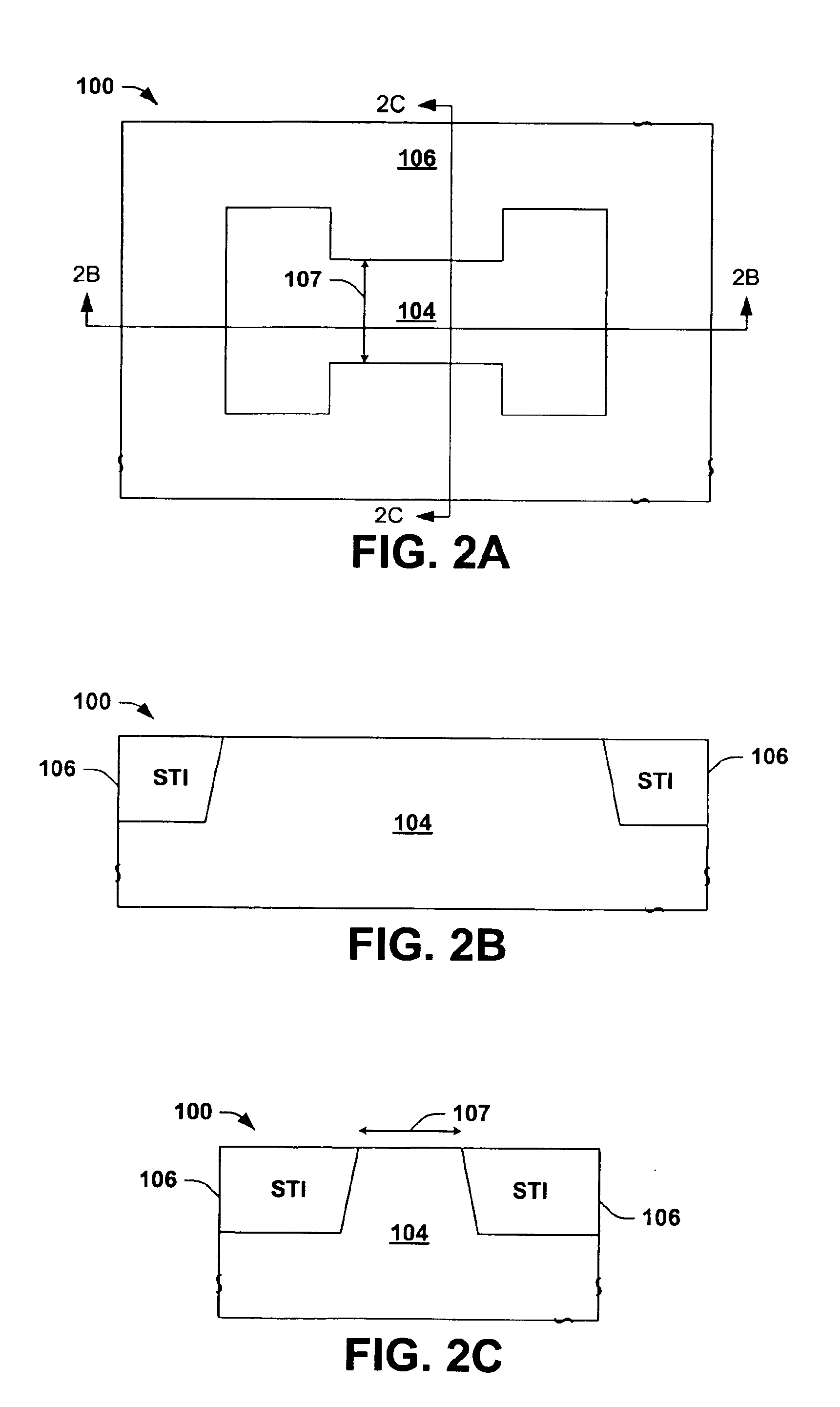
[0020]The present invention will now be described with reference to the attached drawing figures, wherein like reference numerals are used to refer to like elements throughout, and wherein the illustrated structures and devices are not necessarily drawn to scale. The invention relates to transistor devices and fabrication methods wherein a semiconductor body is provided over a starting structure with a semiconductor body dimension that is independent of lithography technology limitations. This allows tuning or optimization of transistor performance, including improved volume inversion in a multi-gate transistor channel, wherein the semiconductor body or thickness can be made smaller than the device gate length, for example, less than half the gate length.

[0021]In the examples illustrated and described below, the semiconductor body is formed in a cavity of a temporary form structure having spacers therein, through deposition of epitaxial silicon or other semiconductor material, where...


PUM


Abstract

Multi-gate MOS transistors and fabrication methods are described, in which the transistor semiconductor body thickness or width is lithography independent, allowing scaled triple and quad-gate devices having semiconductor bodies smaller than a lateral gate length dimension. A form structure is provided over a semiconductor wafer starting structure, and spacers are formed along one or more sidewalls of an opening in the form structure. A semiconductor material is deposited in the opening by epitaxial growth or other deposition process, and the form structure and the spacer are removed. A gate structure is then formed along the top and sides of a central portion of the formed semiconductor body. The spacer may be L-shaped, providing an undercut or recess at the bottom of the semiconductor body sidewall, and the gate may be formed in the undercut area to allow fabrication of more than three gates.

Description

RELATED APPLICATIONS[0001]This application is related to U.S. patent application Ser. No. 10 / 696,539, filed on Oct. 23. 2003, entitle TRIPLE GATE MOSFET TRANSISTOR AND METHODS FOR FABRICATING THE SAME.FIELD OF INVENTION[0002]The present invention relates generally to semiconductor devices and more particularly to multiple-gate MOSFET transistors with lithography independent silicon body thickness and fabrication methods therefor.BACKGROUND OF THE INVENTION[0003]Metal-oxide-semiconductor field-effect transistors (MOSFETs) are widely used in the electronics industry for switching, amplification, filtering, and other tasks related to both analog and digital electrical signals. Conventional planar MOS transistors include a gate dielectric overlying a channel region at the upper surface of a silicon substrate and a gate electrode situated above the gate dielectric. Source and drain regions are formed in the substrate on either lateral side of the channel. In operation, the gate electrode...

Claims


Application Information

Patent Timeline
Patent Type & Authority Patents(United States)
IPC IPC(8): H01L27/148H01L21/02H01L21/3205H01L21/336H01L29/76H01L29/786H01L31/18
CPCH01L29/66553H01L29/66651H01L29/66795H01L29/785H01L29/7853H01L31/18
Inventor CHAMBERS, JAMES JOSEPH
Owner TEXAS INSTR INC
Why Eureka
Try Eureka