Method and structure for transistor with reduced drain-induced barrier lowering and on resistance

Inactive Publication Date: 2014-06-12
GLOBALFOUNDRIES INC
View PDF4 Cites 15 Cited by
  • Summary
  • Abstract
  • Description
  • Claims
  • Application Information

AI Technical Summary

Benefits of technology

[0005]In general, embodiments of the invention provide an improved method and structure for a transistor with reduced DIBL and RON. A sigma cavity is formed in a semiconductor substrate adjacent to a transistor. The sigma cavity is filled with an epitaxially grown semiconductor material that also serves as a stress-inducing region for the purposes of increasing carrier mobility. The epitaxially grown semiconductor material is doped with a reverse doping profile, which is lightly doped at the beginning. A lightly doped region lines the interior

Problems solved by technology

However, smaller critical dimensions often create some performance drawbacks.
In particular, a known category of performance limitations known as short channel effects become more significant as the length of the channel of CMOS devices is reduced.

Method used


Image

  • Method and structure for transistor with reduced drain-induced barrier lowering and on resistance
  • Method and structure for transistor with reduced drain-induced barrier lowering and on resistance
  • Method and structure for transistor with reduced drain-induced barrier lowering and on resistance

Examples


Embodiment Construction

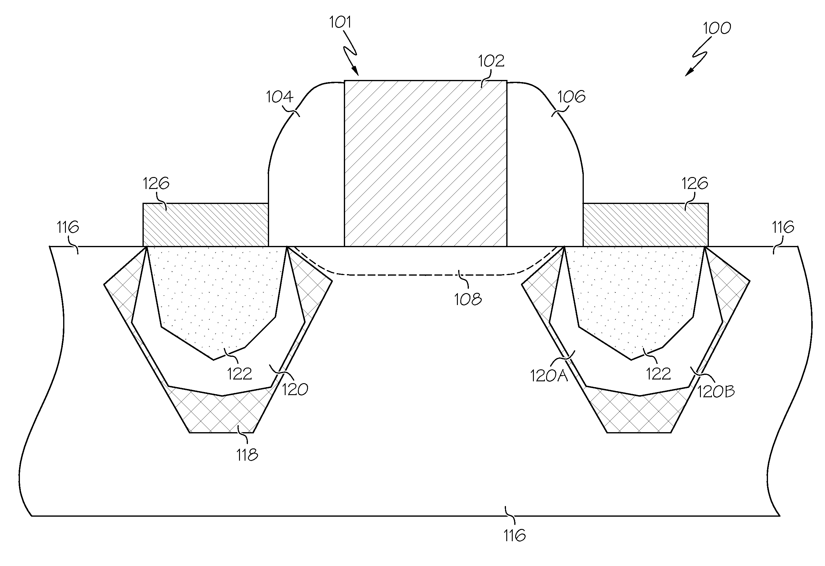
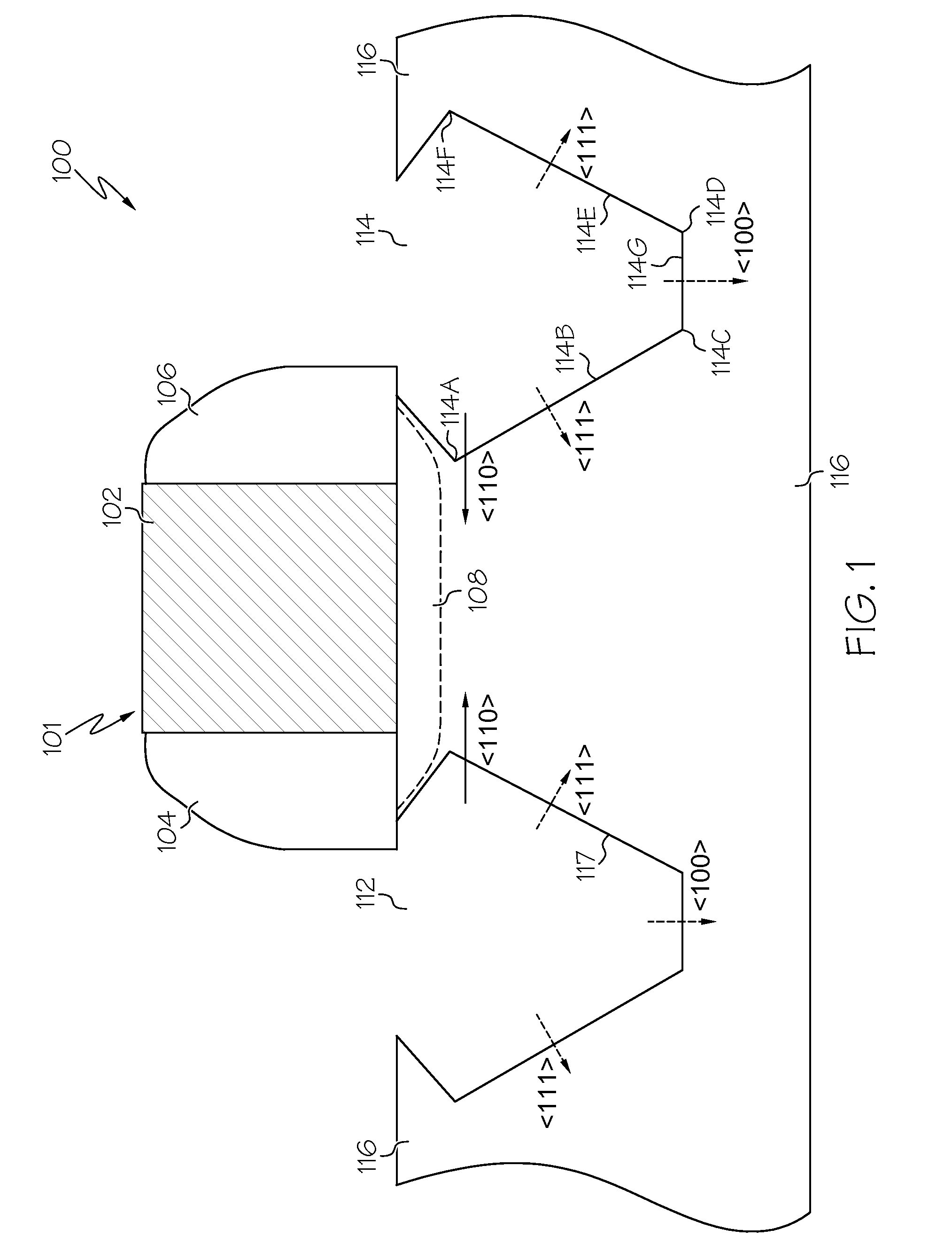
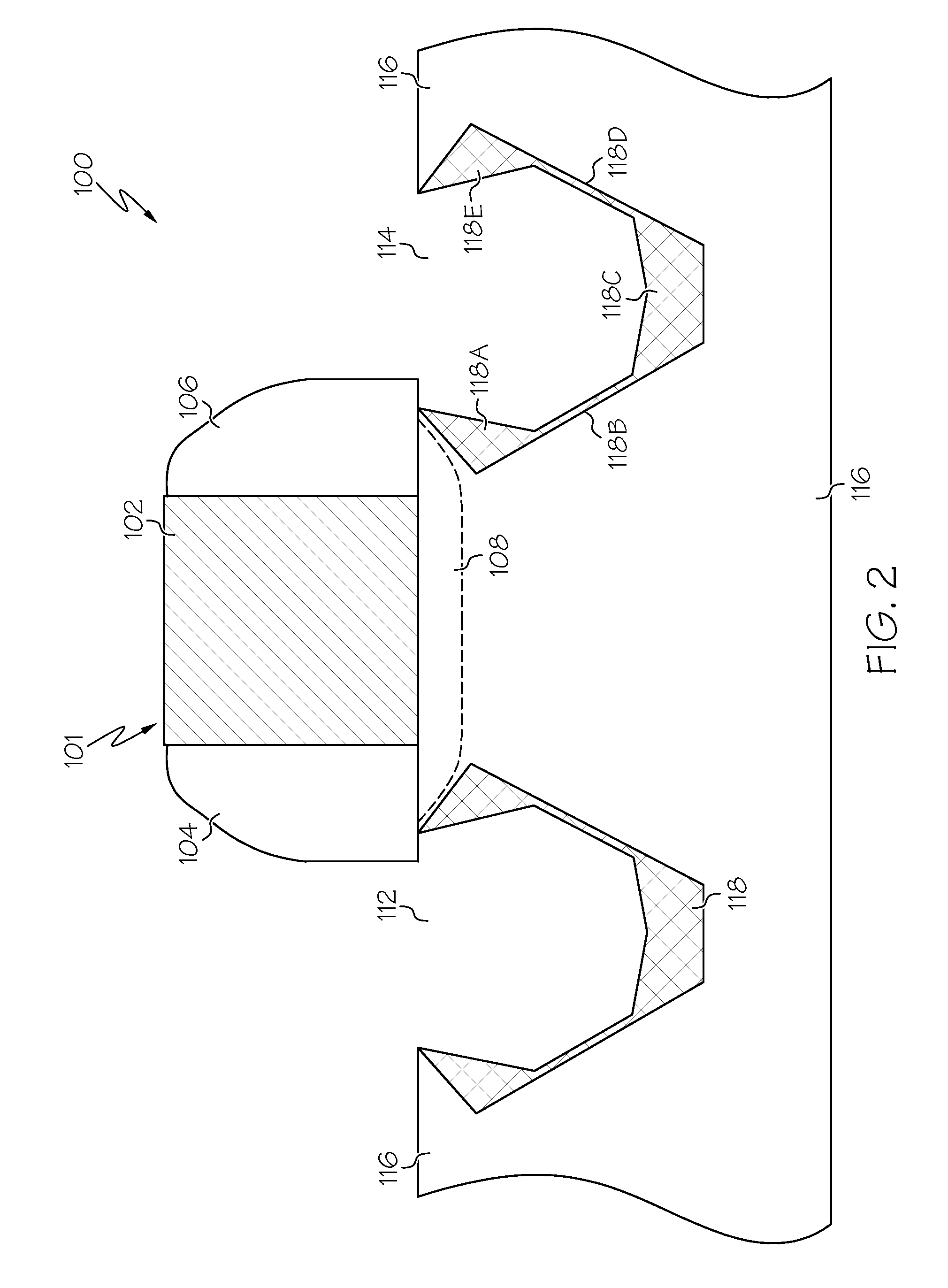
[0017]Exemplary embodiments will now be described more fully herein with reference to the accompanying drawings, in which exemplary embodiments are shown. Exemplary embodiments of the invention provide an improved method and structure for a transistor with reduced DIBL and RON. A sigma cavity is formed in a semiconductor substrate adjacent to a transistor. The sigma cavity is filled with an epitaxially grown semiconductor material that also serves as a stress-inducing region for the purposes of increasing carrier mobility. The epitaxially grown semiconductor material is doped with a reverse doping profile. A lightly doped region lines the interior of the sigma cavity, followed by an undoped region, followed by a heavily doped region. The shape of the lightly doped region is such that it is thicker adjacent to the channel, and thinner below the channel. The shape of the undoped region is such that it is thinner adjacent to the channel and thicker below the channel. Such a combination...


PUM


Abstract

Embodiments of the invention provide an improved method and structure for a transistor with reduced DIBL and RON. A sigma cavity is formed in a semiconductor substrate adjacent to a transistor. The sigma cavity is filled with an epitaxially grown semiconductor material that also serves as a stress-inducing region for the purposes of increasing carrier mobility. The epitaxially grown semiconductor material is doped with a reverse doping profile. A lightly doped region lines the interior of the sigma cavity, followed by an undoped region, followed by a heavily doped region. The shape of the lightly doped region is such that it is thicker adjacent to the channel, which reduces RON, and thinner below the channel, which reduces DIBL.

Description

FIELD OF THE INVENTION[0001]The present invention relates generally to semiconductor fabrication and, more particularly, to a method and structure for a transistor with reduced drain-induced barrier lowering (DIBL) and on resistance (RON).BACKGROUND[0002]The semiconductor fabrication industry has a goal to achieve individual devices with smaller physical dimensions. The trend in the industry is towards thinner device regions and gate oxides, shorter channels, and lower power consumption.[0003]However, smaller critical dimensions often create some performance drawbacks. In particular, a known category of performance limitations known as short channel effects become more significant as the length of the channel of CMOS devices is reduced. One particular short-channel effect in CMOS devices, known as Drain Induced Barrier Lowering (DIBL), is significantly responsible for the degradation of performance in transistor devices. DIBL is a reduction in the potential barrier between the drain...

Claims


Application Information

Patent Timeline
IPC IPC(8): H01L29/78H01L21/02
CPCH01L29/6659H01L29/66636H01L29/7833H01L29/7848
Inventor LIU, JINPINGQI, YIYANG, XIAODONG
Owner GLOBALFOUNDRIES INC
Why Eureka
Try Eureka