Memory heat sink

a heat sink and memory technology, applied in semiconductor devices, semiconductor/solid-state device details, cooling/ventilation/heating modifications, etc., can solve the problems of increased heat dissipation needs, operating errors within devices, and components within semiconductors that do not work properly, so as to achieve enhanced coolant flow, reduce heat dissipation, and reduce the effect of heat loss

Inactive Publication Date:
View PDF13 Cites 112 Cited by
  • Summary
  • Abstract
  • Description
  • Claims
  • Application Information

AI Technical Summary

Benefits of technology

[0006]The present invention provides an apparatus for dissipating heat from a semiconductor device that meets dimensional requirements for the semiconductor device. The apparatus provides a relatively large surface area for transferring heat away from a semiconductor device, and provides for enhanced coolant flow through or around the apparatus.

Problems solved by technology

The generation of heat within semiconductor packages for devices such as microprocessors and memories has long been recognized as a significant source of operating errors of such semiconductor devices.
Operating errors may result from, for example, components within the semiconductor not functioning properly due to operating temperatures becoming too high.
However, if the transistor is operating at a sufficiently high operating temperature, it may be switched on at a lower voltage, resulting in an operating error within the device.
As technology has progressed, heat loads generated from semiconductor devices have risen, resulting in increased need for heat dissipation.
Thus problems arise in effectuating the necessary transfers of heat from increasingly confined spaces.
The maximum width for such a memory component is limited by the space between in-line slots, resulting in a relatively small space allowance and little room for heat dissipation devices.

Method used


Image

  • Memory heat sink
  • Memory heat sink
  • Memory heat sink

Examples


Embodiment Construction

[0014]While the present invention is described with reference to the accompanying drawings, in which one embodiment of the present invention is illustrated, it is to be understood at the outset that persons of skill in the appropriate arts may modify the invention here described while still achieving the favorable results of the invention. Accordingly, the description that follows is to be understood as being a broad disclosure directed to persons of skill in the appropriate arts, and not as limiting upon the present invention.

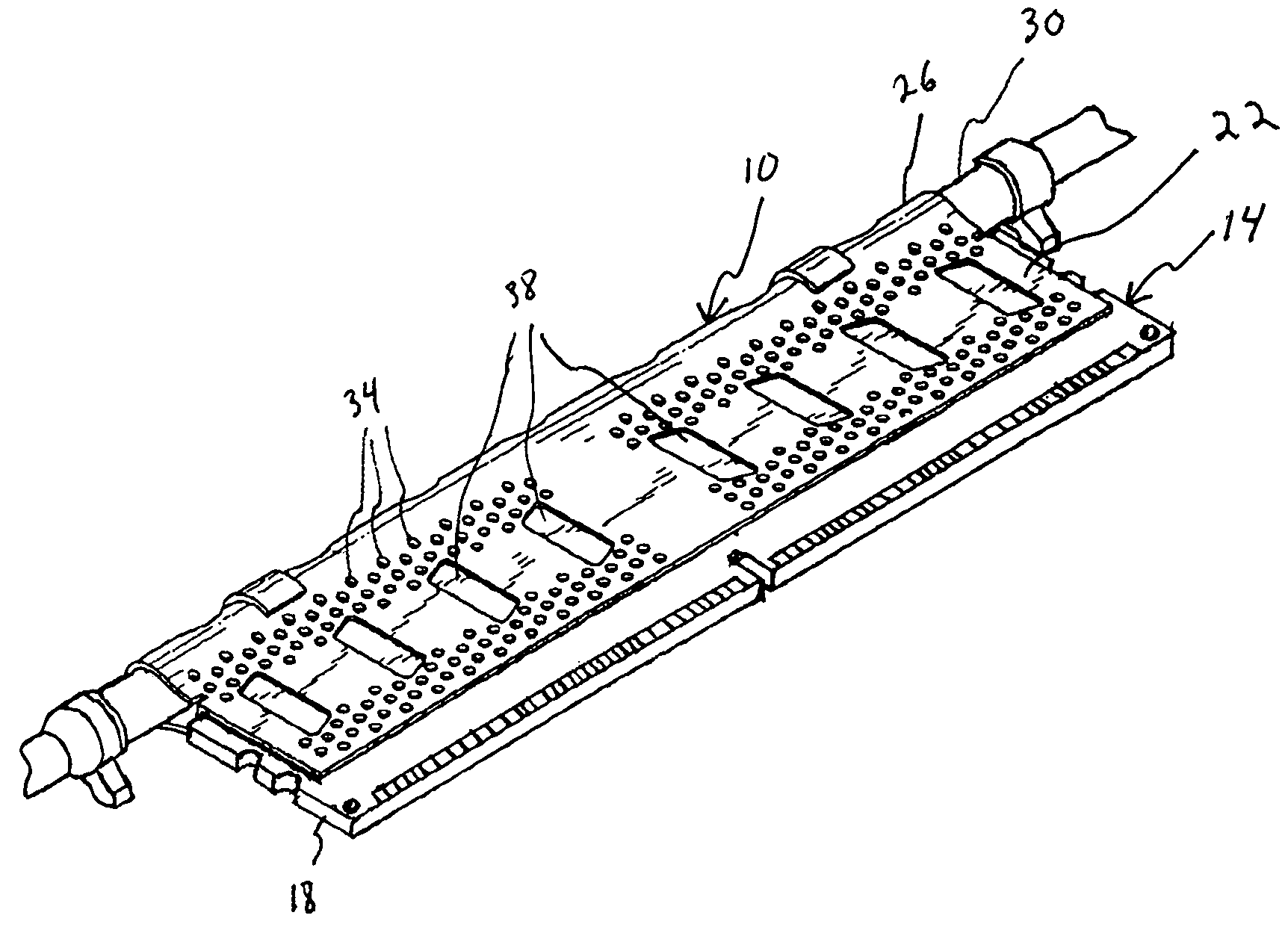
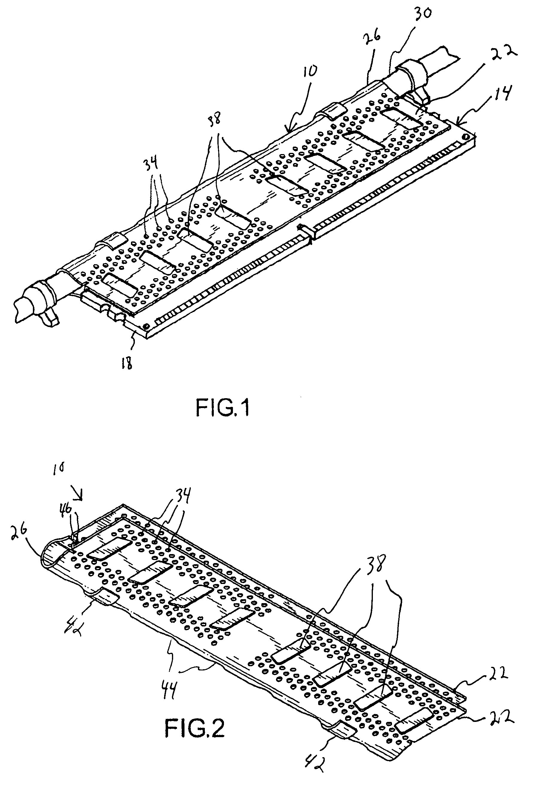
[0015]Referring now FIG. 1, a perspective view of a heat sink 10 of an embodiment of the present invention is described. The heat sink 10 of this embodiment is configured to provide heat dissipation from a memory device 14. As is well known, such a memory device 14 may include, for example, a single inline memory module (SIMM), or a dual inline memory module (DIMM). The memory device 14 includes a number of semiconductor memory components (not shown) on one or...


PUM


Abstract

An apparatus is provided for dissipating heat from a semiconductor device that meets dimensional requirements for the semiconductor device and provides enhanced cooling for the semiconductor device. The apparatus provides a relatively large surface area for transferring heat away from a semiconductor device, and provides for enhanced coolant flow through or around the apparatus. The apparatus includes a channel that may accommodate a heat pipe to further enhance transfer of heat away from the semiconductor device.

Description

CROSS REFERENCE TO RELATED APPLICATIONS[0001]This application is a continuation-in-part of pending U.S. patent application Ser. No. 29 / 216,013, filed on Oct. 28, 2004, titled MEMORY CARD HEAT SINK, incorporated herein by reference as if set out in full.FIELD OF THE INVENTION[0002]The present invention is directed to heat dissipation devices and, more specifically, to a heat spreading device for a memory component of a computing system.BACKGROUND[0003]The generation of heat within semiconductor packages for devices such as microprocessors and memories has long been recognized as a significant source of operating errors of such semiconductor devices. Operating errors may result from, for example, components within the semiconductor not functioning properly due to operating temperatures becoming too high. For example, a transistor within a device may be nominally switched into an “on” state upon the application of a preset voltage. However, if the transistor is operating at a sufficien...

Claims


Application Information

Patent Timeline
Patent Type & Authority Patents(United States)
IPC IPC(8): H05K7/20
CPCH01L23/427H01L23/473H01L2924/0002H01L2924/00
Inventor STATHAKIS, D. GEORGE
Why Eureka
Try Eureka