Method of fabricating no-lead package for semiconductor die with half-etched leadframe

a technology of leadframe and semiconductor die, which is applied in the field of no-lead package, can solve the problems of corroding metal bonds, bond cracking, and separating the bonding compound from the contact, so as to reduce the torque imposed by the saw blade, reduce the amount of heat, and reduce the effect of separation

Inactive Publication Date: 2006-12-26
UTAC HEADQUARTERS PTE LTD
View PDF14 Cites 33 Cited by
  • Summary
  • Abstract
  • Description
  • Claims
  • Application Information

AI Technical Summary

Benefits of technology

[0008]The grooves reduce the torque that is imposed by the saw blade on the structure, and they also reduce the amount of heat that is generated during the sawing process. As explained above, this tends to reduce or eliminate separation between the metal contacts and the plastic molding compound. The secondary grooves also separate the force generated by the cutting action of the saw blade from the bonding wires and areas, thereby preventing cracks in the bonds and bonding wires. The grooves also reduce the size of metal burrs and chips in the molding compound that are created by the sawing process. They also increase the throughput of the process and reduce the wear and tear on the saw blade.

Problems solved by technology

Also, the friction from the saw produces heat, and the differing thermal expansion coefficients of the metal contacts and the molding compound, respectively, likewise tend to cause the molding compound to separate from the contacts.
This moisture may corrode the metal bonds in the package and as the temperature of the package changes cause the bonds to crack and the package to fail.

Method used


Image

  • Method of fabricating no-lead package for semiconductor die with half-etched leadframe
  • Method of fabricating no-lead package for semiconductor die with half-etched leadframe
  • Method of fabricating no-lead package for semiconductor die with half-etched leadframe

Examples


Embodiment Construction

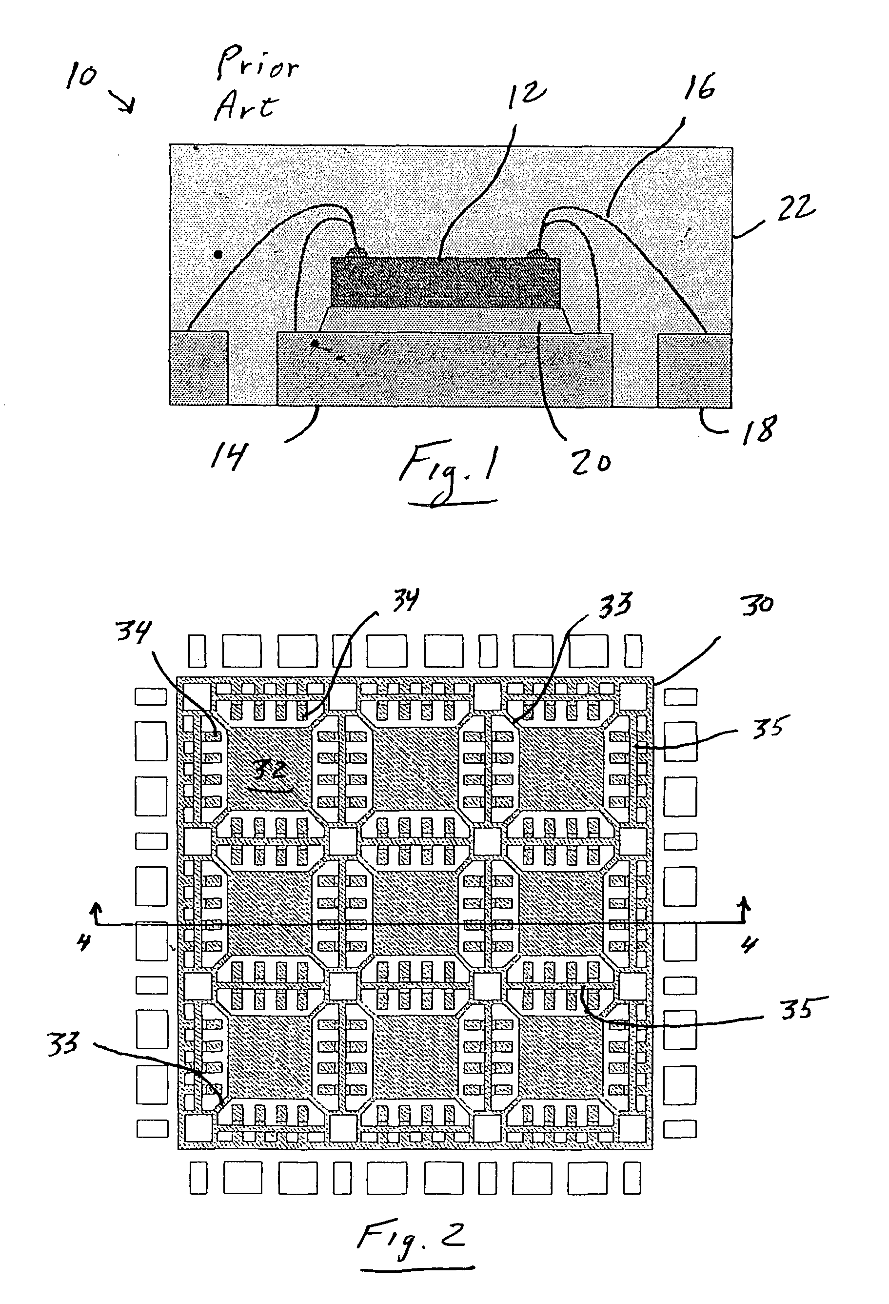
[0022]FIG. 2 shows a matrix array 30 of leadframes for QFN packages. The leadframes in matrix array 30 have nine die-attach pads 32, arranged 3×3, on which semiconductor dice are to be mounted. Each die-attach pad 32 is surrounded by 16 metal contacts 34, four on each side. It will be understood that the leadframe could have more or less than nine die-attach pads and each die-attach pad could be surrounded by more or less than 16 metal contacts. Die-attach pads 32 and contacts 34 are held together by tie bars 33 and 35. Tie bars 33 connect to the corners of die-attach pads 32, and tie bars 35, which are arranged in an orthogonal pattern, connect the contacts 34 together. Tie bars 35 will be severed later when the packages are separated. The open boxes around the periphery of matrix array 30 are “heat slots” used to compensate for the expansion of the copper alloy during the wire bonding and molding processes.

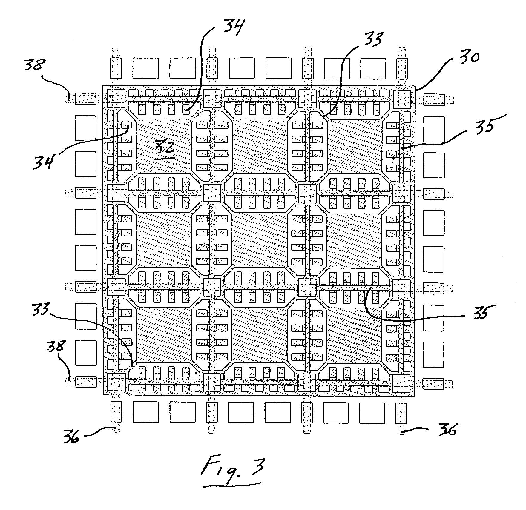
[0023]FIG. 3 is a view similar to FIG. 2 showing orthogonal saw cuts 36 and...


PUM


Abstract

A series of grooves are etched in a leadframe to be used in fabricating a group of semiconductor packages at locations where the leadframe will later be sawed to separate the semiconductor packages. In variations of the process, the grooves may be wider or narrower than the kerf of the saw cuts and may be formed on the side of the leadframe facing towards or away from the entry of the saw blade.

Description

FIELD OF THE INVENTION[0001]This invention relates to packages for semiconductor dice and in particular to “no-lead” packages, i.e., packages in which there are no leads protruding from the surfaces of the package. Instead, electrical contact to external circuitry is made by means of contacts having exposed faces that are flush with the surfaces of the package.BACKGROUND OF THE INVENTION[0002]Semiconductor dice are normally packaged in a plastic capsule to protect them from physical damage. Connections are made to external circuitry, such as a printed circuit board (PCB), by means of metal pieces, called “lead fingers,” that protrude from the capsule and can be soldered or otherwise connected electrically. Alternatively, in a “no lead” package the metal pieces have faces that are flush with the surfaces of the capsule. Two types of “no-lead” packages are designated in the industry as QFN (Quad Flat No Lead) and DFN (Dual Flat No Lead).[0003]A cross-sectional view of a typical “no-le...

Claims


Application Information

Patent Timeline
Patent Type & Authority Patents(United States)
IPC IPC(8): H01L23/495H01L21/60
CPCH01L21/4828H01L21/4842H01L21/561H01L23/49548H01L24/97H01L24/29H01L2224/32245H01L2224/48091H01L2224/48247H01L2224/48465H01L2224/73265H01L2224/85001H01L2224/92H01L2224/92247H01L2224/97H01L2924/01012H01L2924/01015H01L2924/01029H01L2924/0103H01L2924/01082H01L2924/18165H01L2224/83H01L2224/85H01L2924/00014H01L2224/48257H01L2924/00012H01L24/48H01L2924/01006H01L2924/01033H01L2924/3512H01L2924/00H01L2924/181H01L24/73H01L2224/45099H01L2224/45015H01L2924/207
Inventor SIRINORAKUL, SARAVUTHNONDHASITTHICHAI, SOMCHAIJEWJAITHAM, SITTACHUA, YEE HEONG
Owner UTAC HEADQUARTERS PTE LTD
Why Eureka
Try Eureka