Method and apparatus for pixel signal binning and interpolation in column circuits of a sensor circuit

a column circuit and sensor technology, applied in the field of image sensors, can solve the problems of reducing the overall power requirements of the sensor, and achieve the effects of reducing the signal bandwidth, reducing the overall power requirements of the sensor, and reducing the aliasing

Inactive Publication Date: 2006-12-26
ROUND ROCK RES LLC
View PDF10 Cites 54 Cited by
  • Summary
  • Abstract
  • Description
  • Claims
  • Application Information

AI Technical Summary

Benefits of technology

[0008]In general, embodiments of the invention provide an imaging circuit, system, and related methods for incorporating signal binning into the readout circuitry. Binning is defined as accumulating or interpolating the charge of multiple pixels and reading them out in a single operation. By incorporating binning into the readout circuitry, various sub-resolution processes can be implemented to minimize aliasing effects. Additionally, by using analog processing for the binning, signal bandwidth may be reduced. This in turn reduces the overall power requirements of the sensor. An additional benefit to using analog binning is that the signal-to-noise ratio (SNR) advantages achieved from binning are more pronounced in the analog domain than they are in the digital domain.

Problems solved by technology

This in turn reduces the overall power requirements of the sensor.

Method used


Image

  • Method and apparatus for pixel signal binning and interpolation in column circuits of a sensor circuit
  • Method and apparatus for pixel signal binning and interpolation in column circuits of a sensor circuit
  • Method and apparatus for pixel signal binning and interpolation in column circuits of a sensor circuit

Examples


Embodiment Construction

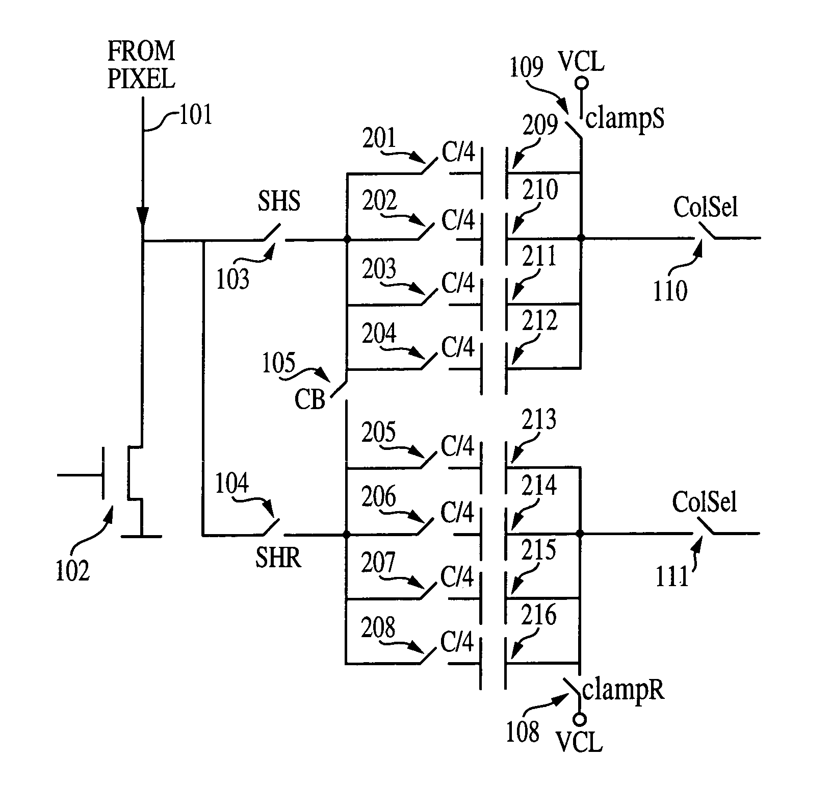
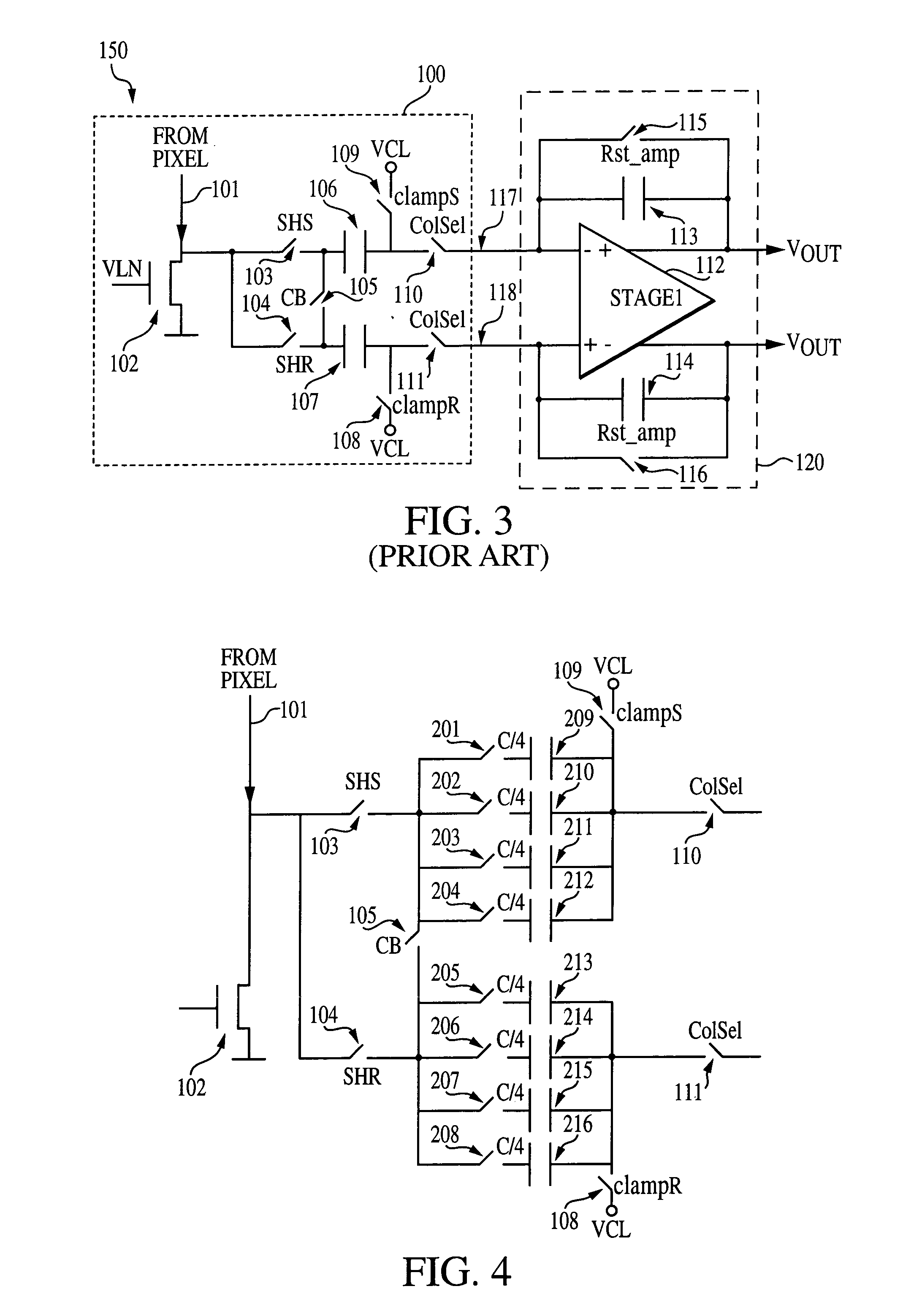
[0030]FIG. 3 illustrates a differential charge-domain readout circuit 150 for an image sensor, wherein a column readout circuit 100 receives a signal from a pixel along a column line 101. Examples of such circuitry may be found in commonly-assigned U.S. Pat. No. 6,222,175, which is incorporated by reference in its entirety herein. The readout circuit 100 includes a load transistor 102 that receives a signal (VLN) at its gate. As is known in the art, the VLN signal activates the load transistor 102 such that it provides a load on the column line 101. The column line 101 is further coupled to two sample-and-hold circuits for storing a pixel signal level when a first sample-and-hold signal (SHS) is applied and a reset level when a second sample-and-hold signal (SHR) is applied to the readout circuit 150. Sampling both the reset and pixel signal levels allows correlated double sampling (CDS) to be performed, which can reduce reset noise associated with the connected pixel as well as noi...


PUM


Abstract

A binning circuit and related method, wherein pixel signals from column circuits in a sensor circuit are sampled and interpolated. The binning circuit samples analog pixel and reset signals from different sensor circuit column lines. Once a predetermined number of column lines are sampled in the binning circuit, the sampled pixel signals are averaged together in one operation, while the reset signals are averaged together in another operation.

Description

FIELD OF THE INVENTION[0001]The present invention relates generally to image sensors, and, in particular, to charge-domain analog readout circuits for such sensors.BACKGROUND OF THE INVENTION[0002]Image sensors find applications in a wide variety of fields, including machine vision, robotics, guidance and navigation, automotive applications, and consumer products. In many smart image sensors, it is desirable to integrate on-chip circuitry to control the image sensor and to perform signal and image processing on the output image. Unfortunately, charge-coupled devices (CCD), which have been one of the dominant technologies used for image sensors, do not easily lend themselves to large scale signal processing and are not easily integrated with CMOS circuits. Moreover, a CCD is read out by sequentially transferring the signal charge through the semiconductor, and the readout rate is limited by the need for nearly perfect charge transfer.[0003]Active pixel sensors (APS), which have one o...

Claims


Application Information

Patent Timeline
Patent Type & Authority Patents(United States)
IPC IPC(8): H01L27/00H04N5/217H04N5/347H04N5/363H04N5/365H04N5/374H04N5/378
CPCH04N5/347H04N3/1562H04N25/46
Inventor KRYMSKI, ALEXANDER
Owner ROUND ROCK RES LLC
Why Eureka
Try Eureka