Insulated gate transistor incorporating diode

a technology of insulating gate transistor and diode, which is applied in the field of transistors, can solve the problems of reducing the performance of an igbt, the conductible current of the power mosfet is relatively low, and the power mosfet is unsuitable for high current applications, and achieves the effect of improving the recovery characteristics of the diod

Active Publication Date: 2006-12-26
MITSUBISHI ELECTRIC CORP
View PDF24 Cites 32 Cited by
  • Summary
  • Abstract
  • Description
  • Claims
  • Application Information

AI Technical Summary

Benefits of technology

[0019]It is an object of the present invention to effectively improve recovery characteristics of a diode (be also referred to as a diode portion) which serves as a FWD and is incorporated in an insulated gate transistor (an IGBT, a vertical MOSFET or the like) having a trench gate structure, to thereby overcome the above-described technological frustration.
[0030]The subject matter of the present invention lies in provision of the first side diffusion region for each of insulated gate transistor units (for example, IGBT units or vertical MOSFET units). This reduces an amount of carriers injected from the first semiconductor layer during an operation of a diode portion (which includes the first main electrode, the first semiconductor layer, the semiconductor substrate, the fourth semiconductor layer and the second main electrode) incorporated in each of the units, to thereby significantly improve recovery characteristics of the diode portion functioning as a built-in FWD.

Problems solved by technology

Instant release of the energy stored in the L of the motor leads to generation of an electric power which is high enough to degrade performance of an IGBT.
However, a density of a conductible current of the power MOSFET is relatively low, and thus the power MOSFET is unsuitable for high current applications.
Such voltage is too high for a breakdown voltage of a built-in freewheeling diode.
Because of this high breakdown voltage, a barrier which is unsuitable as a freewheeling diode is formed, and thus performance of the IGBT is significantly degraded due to heat generated by the high breakdown voltage applied during freewheeling.
For this reason, while an IGBT is advantageous to a power MOSFET in that flow of a high current in a device is permitted, an IGBT still has a disadvantage of requiring a distinct freewheeling diode connected to the IGBT when the IGBT is employed as a switching device of an inverter circuit, in view of its circuitry.
In high current applications, as injection of holes from a highly doped base layer is dominant during recovery of the diode, the structure taught in JP No. 6-196705 could not be so effective in improving recovery characteristics.
It is noted that to simply increase the width of the base layer would cause degradation of characteristics about a reverse leakage current and a reverse breakdown voltage.
As a conclusion, the teachings of JP No. 6-196705 cannot be deemed to be effective in improving recovery characteristics of a built-in FWD.

Method used


Image

  • Insulated gate transistor incorporating diode
  • Insulated gate transistor incorporating diode
  • Insulated gate transistor incorporating diode

Examples


Embodiment Construction

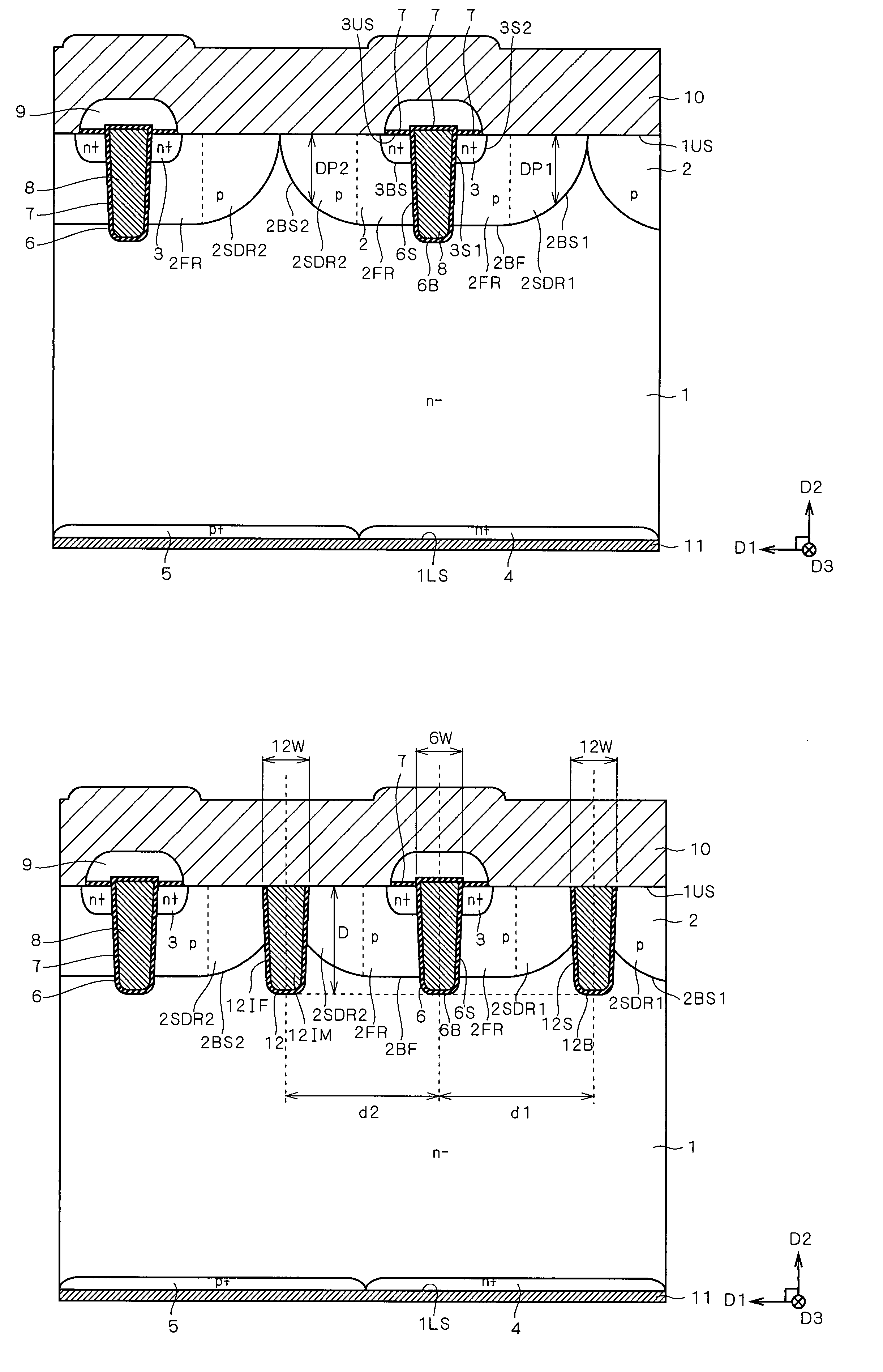
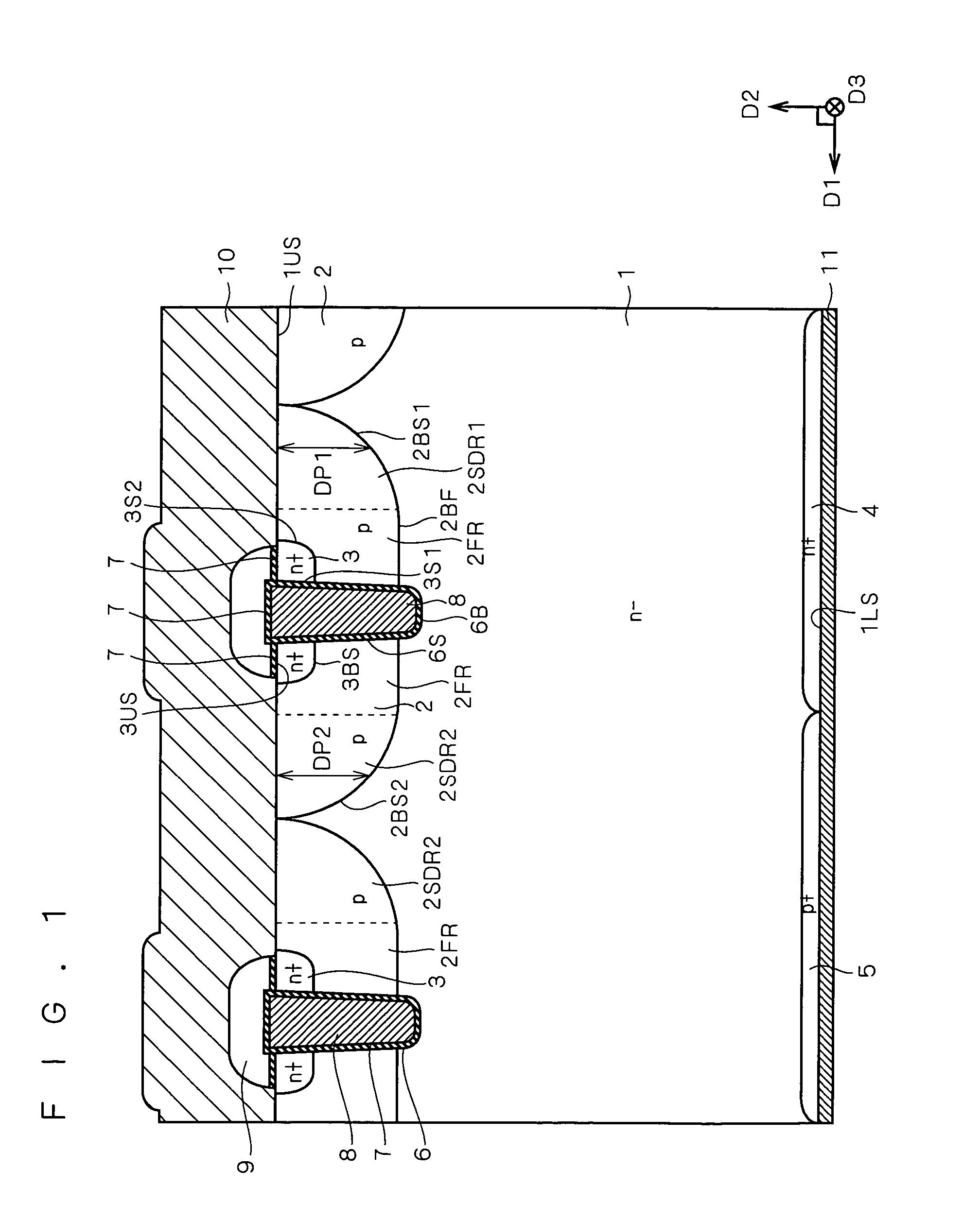
[0068]The following description will be made about a case where each of subject matters of the present invention is applied to an IGBT device of a trench gate type. However, it should be noted that each of technical concepts which will be clarified from the following description in each of various preferred embodiments of the present invention is basically applicable to a vertical MOSFET with a trench gate structure also, as described in detail below.

[0069]First Preferred Embodiment

[0070]Features or essences of one IGBT unit (which includes one IGBT unit cell and a diode incorporated therein) of an IGBT device of a trench gate type according to a first preferred embodiment can be understood by reference to a longitudinal sectional view of FIG. 1 about which details will be provided later. The one IGBT unit includes: I) a first semiconductor layer (a p-type base layer or p-type base region in an example given in the present description) 2 of a second conductivity type (p-type in the ...


PUM


Abstract

A p-type base layer shaped like a well is formed for each of IGBT cells, and a p+-type collector layer and an n+-type cathode layer are formed on a surface opposite to a surface on which the p-type base layer is formed so as to be situated just below the p-type base layer. The p-type base layer of each of the IGBT cells includes a flat region including an emitter region and a bottom surface penetrated by a main trench, and first and second side diffusion regions between which the flat region is interposed. The first side diffusion region is situated just above the n+-type cathode layer and each of the bottom surfaces of the side diffusion regions forms a parabola-shaped smooth curve in longitudinal section. By replacing the p+-type collector layer with the n+-type cathode layer, it is possible to apply features of the above structure to a power MOSFET.

Description

BACKGROUND OF THE INVENTION[0001]1. Field of the Invention[0002]The present invention relates to a transistor including an insulated gate (MOS structure) (for example, an insulated gate bipolar transistor, a power MOSFET or the like). Additionally, an insulated gate bipolar transistor will hereinafter be also referred to as an “IGBT”, and may be also referred to as a “reverse conducting IGBT”. The present invention relates more particularly to a structure of an insulated gate transistor which has a trench gate structure and incorporates a diode functioning as a freewheeling diode (which will hereinafter be also abbreviated as a “FWD”), and a technique for manufacturing the same. The present invention provides for improvement of recovery characteristics exhibited by the diode incorporated in an insulated gate transistor during an operation mode of the diode.[0003]2. Description of the Background Art[0004]In power electronics for driving a motor or the like, under a condition that a r...

Claims


Application Information

Patent Timeline
Patent Type & Authority Patents(United States)
IPC IPC(8): H01L29/76H01L21/28H01L21/331H01L21/336H01L27/04H01L29/06H01L29/41H01L29/739H01L29/78H02M7/5387
CPCH01L29/0696H01L29/1095H01L29/407H01L29/66348H01L29/7397H01L29/7803H01L29/7805H01L29/7806H01L29/7813H01L29/7812H01L2924/13055
Inventor TAKAHASHI, HIDEKI
Owner MITSUBISHI ELECTRIC CORP
Why Eureka
Try Eureka