Optical element for enhanced transmission of light and suppressed increase in temperature

a technology of optical elements and temperature reduction, applied in the field of optical elements, can solve the problems of reducing reliability, difficult to obtain a sufficient intensity of light required for writing data on the optical recording medium, etc., and achieve the effects of suppressing temperature increase, increasing power of light beams, and increasing power

Inactive Publication Date: 2006-12-26
NEC CORP
View PDF14 Cites 22 Cited by
  • Summary
  • Abstract
  • Description
  • Claims
  • Application Information

AI Technical Summary

Benefits of technology

[0028]An object of the present invention is to provide an optical element structure allowing an increased power density of light passing through a subwavelength aperture surrounded by a surface topography on a conductive film while suppressing an increase in temperature caused by an increased power of incident light.
[0029]According to the present invention, the size of a light beam applied to a periodic surface topography on a conductive film and the period of the periodic surface topography are determined so as to maximize a light power efficiency of output light transmitted through the aperture with respect to a reference input light.
[0035]According to another aspect of the present invention, a layer of optical material having a refractive index higher than that of the optical element body is provided on at least one of the first and second surfaces of the conductive film. The addition of this layer reduces the lattice constant required for operation at a given wavelength and therefore decreases the total irradiation area necessary to obtain a given transmission enhancement. The optical material may include at least one selected from a group consisting of titanium oxide, zirconium oxide, tantalum oxide, alumina, silicon nitride, and silicon.
[0045]As described above, the diameter of the focused light beam on the first surface of the conductive film and the period of the periodic surface topography are determined so that a power ratio of aperture-transmitted light to the incident light beam is greater than that of aperture-transmitted light which would be obtained if no periodic surface topography is provided in the conductive film. Such an optical element structure allows an increased power density of light passing through the sub-wavelength aperture surrounded by the periodic surface topography on the conductive film while suppressing increase in temperature caused by an increased power of the light beam.

Problems solved by technology

However, the laser light is subject to substantial attenuation during propagation to the sub-wavelength aperture and thereby it is difficult to obtain a sufficient intensity of light required for writing data on the optical recording medium.
Further, the application of an increased power of incident light to the conductive film causes the conductive film and the surface of the optical recording medium adjacent thereto to increase in temperature, resulting in decreased reliability.

Method used


Image

  • Optical element for enhanced transmission of light and suppressed increase in temperature
  • Optical element for enhanced transmission of light and suppressed increase in temperature
  • Optical element for enhanced transmission of light and suppressed increase in temperature

Examples


first embodiment

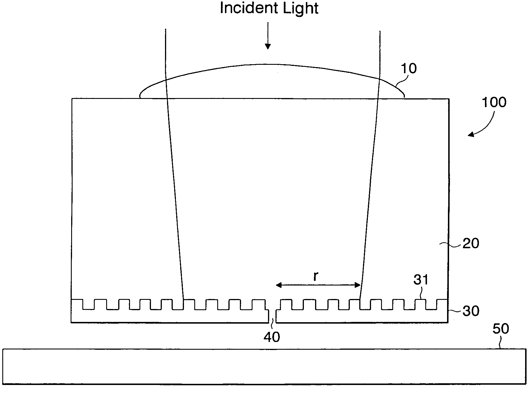
[0078]Referring to FIG. 6, an optical element 100 according to a first embodiment of the present invention is provided with a focus lens 10, an optical element body 20, and a conductive film 30. The optical element 100 is placed near an optical recording medium 50. The focus lens 10 is in contact with the optical element body 20 or may be separately provided. The optical element body 20 is made of transparent material such as optical glass or quartz.

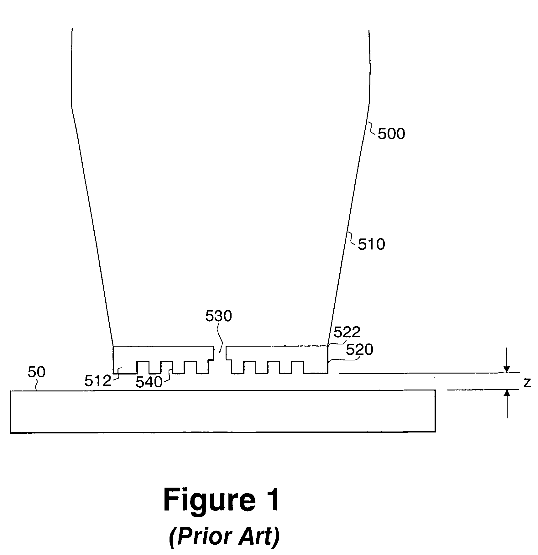
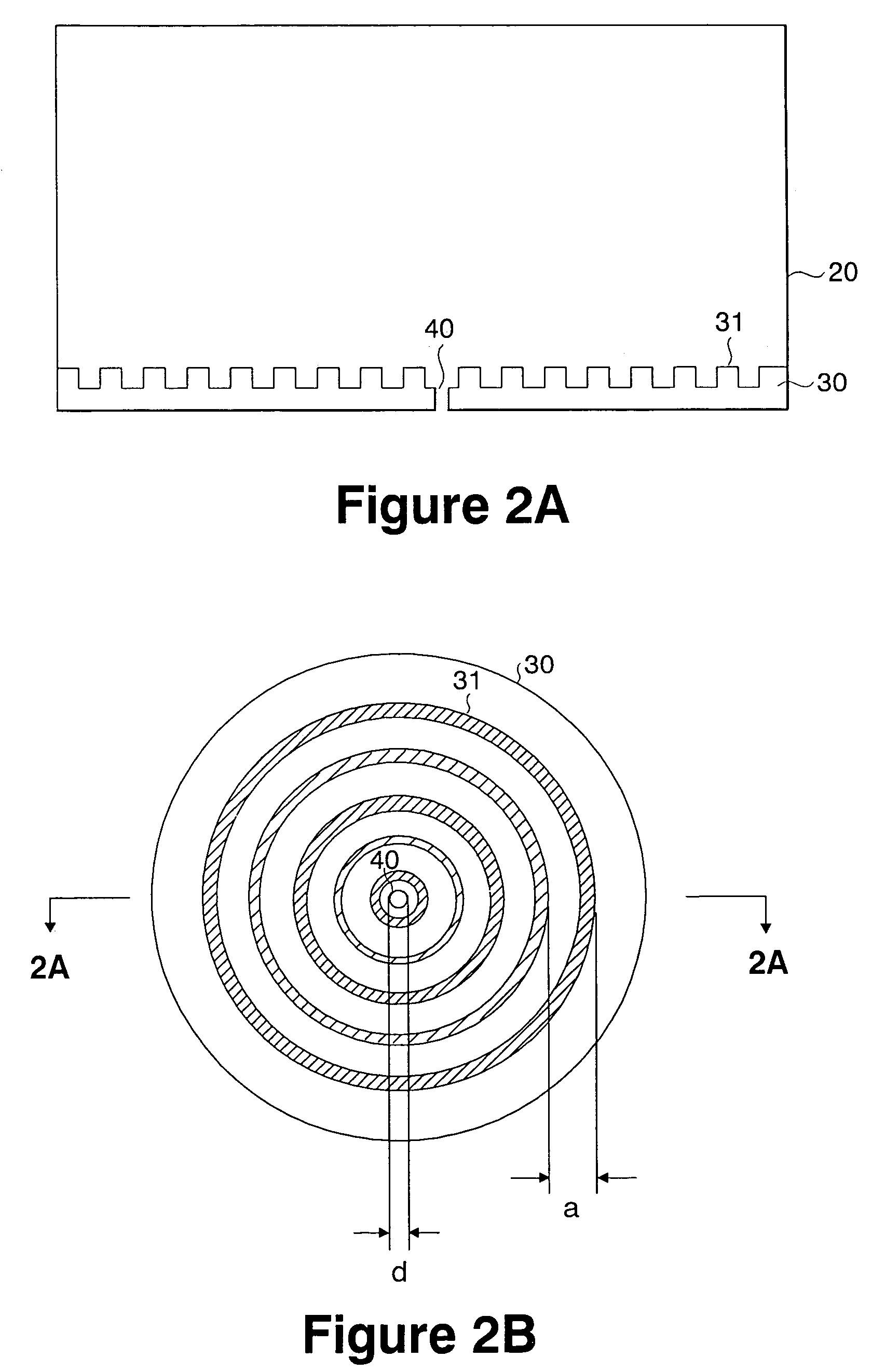
[0079]The conductive film 30 is provided on an end surface of the optical element body 20, the end surface being placed near the optical recording medium 50. The conductive film 30 is made of metal such as silver or doped semiconductor and has an aperture 40 perforating through. The shape of the aperture is described in U.S. application Ser. No. 10 / 098,970, incorporated herein by reference. As described before, the exit size of the aperture 40 determines the resolution of an optical device. The diameter d of the aperture 40 is preferably...

second embodiment

[0089]Referring to FIG. 7, an optical element 100 according to a second embodiment of the present invention is provided with a focus lens 10, an optical element body 20, a high-refractive-index material film 60, and a conductive film 30. The optical element 100 is placed near an optical recording medium 50. The focus lens 10 is in contact with the optical element body 20 or may be separately provided. The optical element body 20 is made of transparent material such as optical glass or quartz.

[0090]The high-refractive-index material film 60 is provided on an end surface of the optical element body 20, the end surface being placed near the optical recording medium 50. The high-refractive-index material film 60 is made of a material having a refractive index higher than that of the optical element body 20, for example, a metal oxide such as titanium oxide or semiconductor such as silicon. Further, the conductive film 30 is deposited on the high-refractive-index material film 60. In ord...

third embodiment

[0098]Referring to FIG. 8, a third embodiment of the present invention is different from the second embodiment as shown in FIG. 7 in that the high-refractive-index material film 60 is provided on one surface of the conductive film 30, which faces the optical recording medium 50. Since materials and the main structure employed in the third embodiment are similar to those in the second embodiment, members similar to those described with reference to FIG. 7 are denoted by the same reference numerals and the details are omitted.

[0099]The high-refractive-index material film 60 may employ a multi-layer structure composed of two or more layers made of different materials.

[0100]It is possible to provide an interface layer between the high-refractive-index material film 60 and the conductive film 30 to achieve improved adhesion and reliability. In this case, it is preferable that the thickness of the interface layer is sufficiently smaller than the penetration depth of the surface plasmon fi...


PUM

PropertyMeasurementUnit
lengthaaaaaaaaaa
lengthaaaaaaaaaa
depthaaaaaaaaaa

Abstract

An optical element structure allowing an increased power density of aperture-transmitted light while suppressing increase in temperature is disclosed. A conductive film has a sub-wavelength aperture formed therein and a periodic surface topography formed thereon. A lens focuses light onto the periodic surface topography with a predetermined diameter. The predetermined diameter of incident light on the conductive film and a period of the periodic surface topography are determined so that a power ratio of aperture-transmitted light to the light beam is greater than that of aperture-transmitted light which would be obtained if no periodic surface topography is provided in the conductive film.

Description

BACKGROUND OF THE INVENTION[0001]1. Field of the Invention[0002]The present invention relates to an optical element provided with a conductive film having a subwavelength aperture and a surface topography formed therein, an optical head and optical data recording / reading apparatus using the optical element.[0003]2. Description of the Related Art[0004]An optical recording medium, such as a CD-ROM (Compact Disk-Read Only Memory) or DVD (Digital Video Disk), has various advantages including the capability of storing large quantities of data, compact design, portability, and robustness. As recording media and data recording / reading apparatuses drop in price, such an optical recording medium becomes increasingly attractive. The data density in optical recording media is desirably higher particularly for storing long-playing video data.[0005]It is known well that the data density in optical recording media is determined by the size of pits on the optical recording medium, which is limited...

Claims


Application Information

Patent Timeline
Patent Type & Authority Patents(United States)
IPC IPC(8): G11B11/00G11B7/00G02F1/01G11B7/12G11B7/135G11B11/105
CPCB82Y10/00G11B7/1203G11B7/1353G11B7/1384G11B7/1387G11B7/122G11B7/1369G02F1/01
Inventor NAKADA, MATSAFUMITHIO, TINEKE
Owner NEC CORP
Why Eureka
Try Eureka