Piezoelectric device

a piezoelectric device and piezoelectric technology, applied in turn-sensitive devices, generators/motors, instruments, etc., can solve the problems of reducing the thickness and the plane the size of the piezoelectric device becomes large, and the inability to achieve miniaturization, so as to prevent the outflow of adhesives and prevent the flow of adhesives

Active Publication Date: 2007-01-02
SEIKO EPSON CORP
View PDF8 Cites 34 Cited by
  • Summary
  • Abstract
  • Description
  • Claims
  • Application Information

AI Technical Summary

Benefits of technology

[0008]A piezoelectric device according to the invention is characterized in that an IC chip is mounted on an inner bottom surface of a package, and a piezoelectric vibrating reed is electrically and mechanically connected onto a TAB tape in which a lead is provided on a surface of a resin tape. The TAB tape to which the piezoelectric vibrating reed has been joined is mounted in the package, whereby the piezoelectric vibrating reed is arranged above the IC chip. In this case, the IC chip includes at least a circuit for driving the piezoelectric vibrating reed, and a circuit for detecting a signal outputted from the piezoelectric vibrating reed. Since the piezoelectric vibrating reed can be arranged above the IC chip, the plane size of the piezoelectric device can be miniaturized. Therefore, the space where the piezoelectric device is mounted on a mounting substrate can be reduced.
[0009]Further, the piezoelectric device is characterized in that the TAB tape has a device hole in its center, and the lead is protruded inward of the device hole. The leading end portion of the lead and a connection electrode provided for the piezoelectric vibrating reed are electrically and mechanically connected. Even if the device hole is provided in the center portion of the TAB tape, because the IC chip is mounted on the inner bottom surface of the package, the piezoelectric vibrating reed can be arranged above the IC chip so that the plane size of the piezoelectric device can be miniaturized. Further, since the TAB tape is joined to the piezoelectric vibrating reed, the elements for calculation can be reduced when the resonance design of the TAB tape is performed. As such, the resonance design can be performed exactly.
[0010]Further, the piezoelectric device is characterized in that the piezoelectric vibrating reed has in its center a base portion on which the connection electrode is formed. A drive arm and a detection arm for detecting an angular velocity are protruded from the base portion. Hereby, the piezoelectric device can be function as a gyro sensor that detects the angular velocity. Further, even if the piezoelectric vibrating reed has the base portion in its center, the piezoelectric vibrating reed can be mounted in the center of the TAB tape. Therefore, the plane size of the piezoelectric device can be miniaturized.
[0011]Further, the piezoelectric device is characterized in that a seal hole through which the inside of the package is air-tightly sealed is provided at the bottom of the package, and the seal hole has a bending portion. If an adhesive flows out from a mount electrode and flows in the seal hole, the adhesive flows out along the side surface of the seal hole. However, due to the bending portion provided for the seal hole, it is possible to prevent the adhesive from flowing to the rear surface of the package. Further, even if a sealant arranged in the seal hole melts, due to the bending portion, it is possible to prevent the sealant from flowing in the inside area of the package where the IC chip or the TAB tape is arranged.
[0012]Further, the piezoelectric device is characterized in that the seal hole includes an outer seal hole located on the outside of the package in relation to the bending portion, and an inner seal hole located on the inside of the package in relation to the bending portion. The outer seal hole and the inner seal hole are separate in the horizontal direction. Since the outer seal hole and the inner seal hole are separate in the horizontal direction, it is possible to prevent the adhesive flowing out from the inner hole from directly dropping in the outer hole. Further, due to the bending portion, the outflow of the adhesive can be prevented. Further, even if a sealant arranged in the seal hole melts, due to the bending portion, it is possible to prevent the sealant from flowing in the inside area of the package where the IC chip or the TAB tape is arranged.

Problems solved by technology

However, when an electronic apparatus on which the piezoelectric device is mounted is minaturized, it is necessary to reduce the thickness and the plane size of the piezoelectric device.
Therefore, the plane size of the piezoelectric device becomes large and the miniaturization cannot be achieved, so that the mounted space of the piezoelectric device becomes large.
Further, if the gyro sensor in which the piezoelectric vibrating reed is mounted on the TAB tape, there is a possibility that the wiring pattern of the TAB tape and the base plate thereof resonate due to a bending vibration of the piezoelectric vibrating reed.
Though a resonation design may be obtained by calculation, the calculation becomes very complicated if the IC chip is mounted on the TAB tape.

Method used


Image

  • Piezoelectric device
  • Piezoelectric device
  • Piezoelectric device

Examples


Embodiment Construction

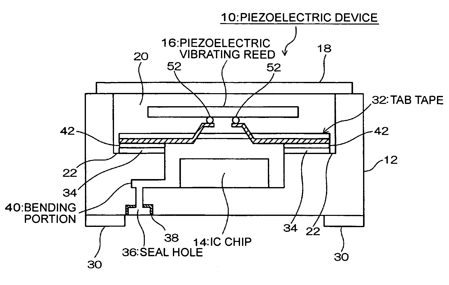
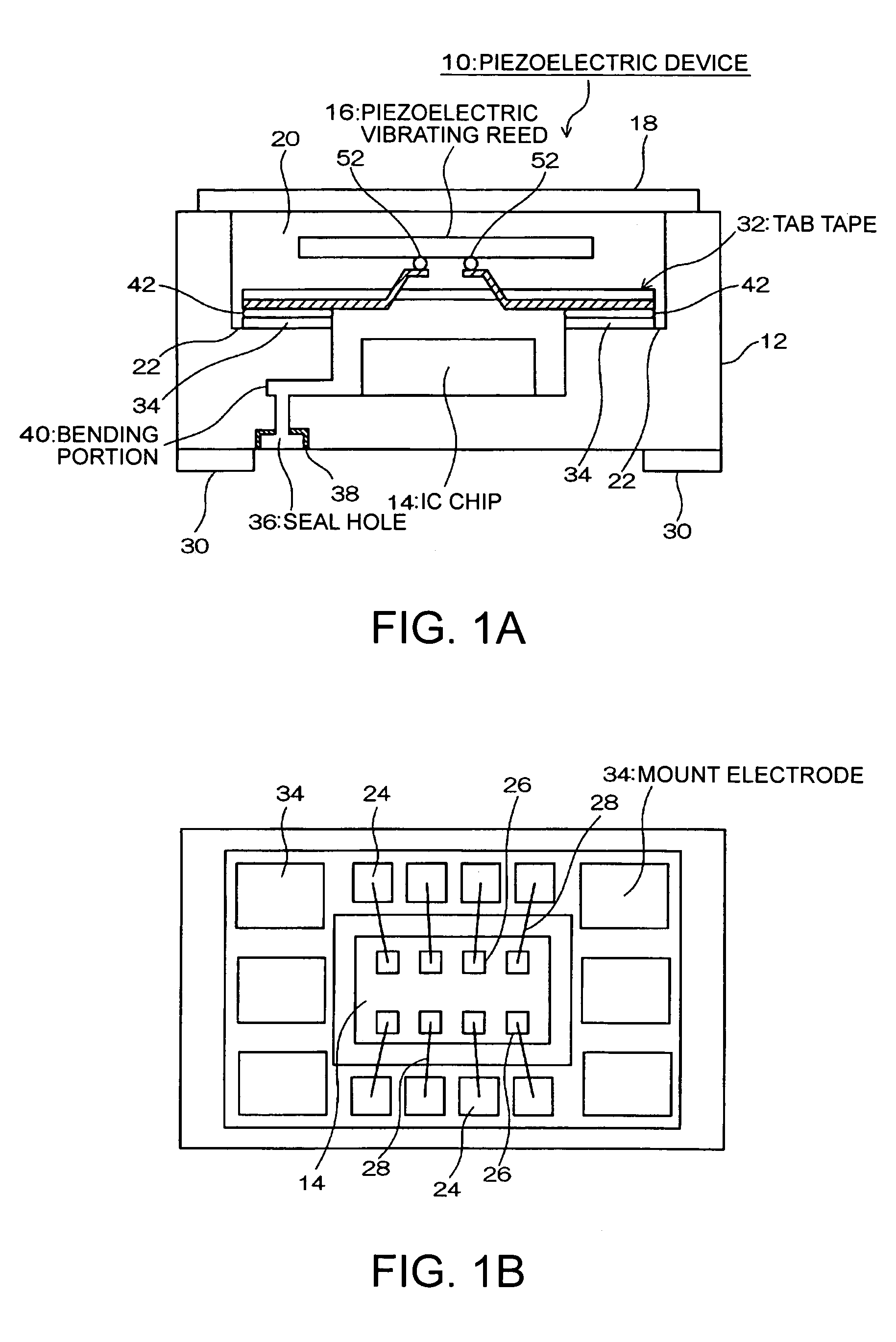
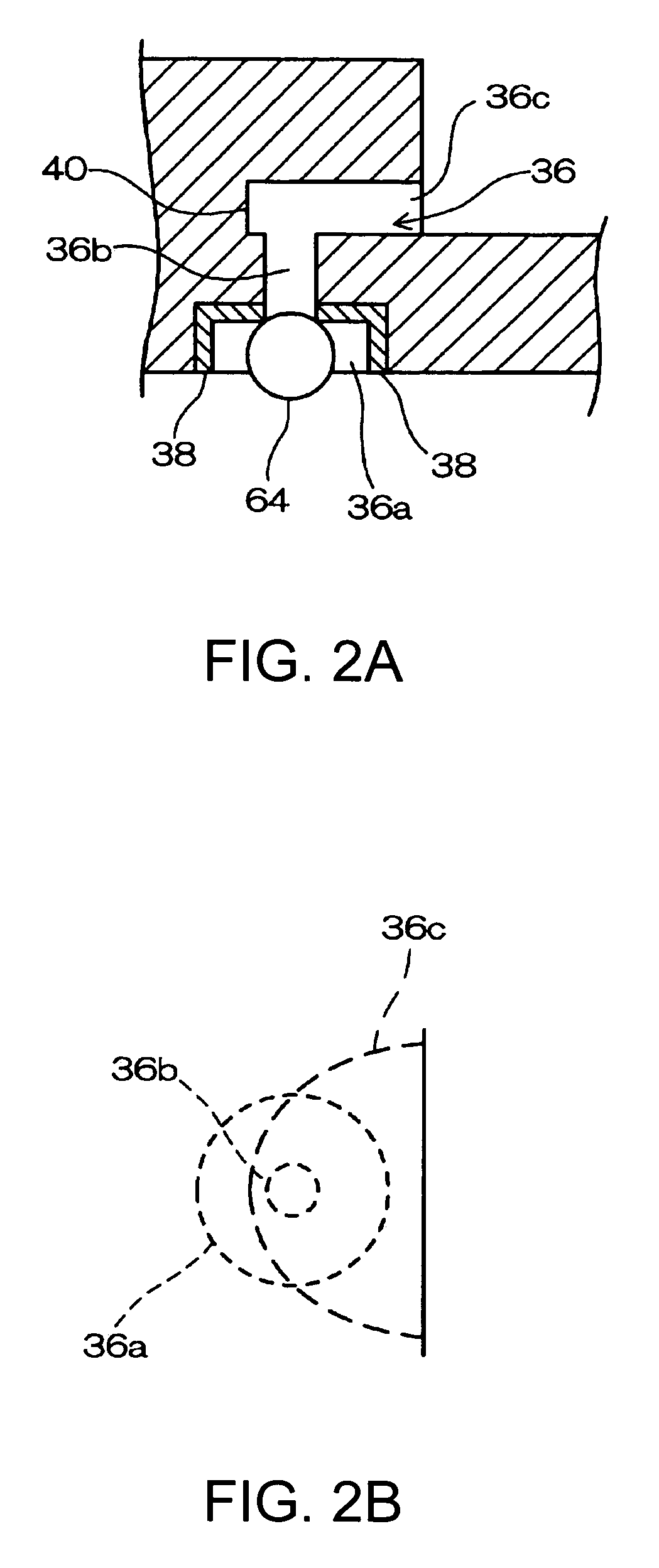
[0022]A piezoelectric device according to the present invention will now be described below. FIG. 1 is an explanatory view of a piezoelectric device, in which FIG. 1(a) is a schematic sectional view, and FIG. 1(b) is a schematic plan view in which a lid and a TAB tape are removed. FIG. 2 is an explanatory view of a seal hole, in which FIG. 2(a) is a schematic sectional view, and FIG. 2(b) is a schematic plan view. FIG. 3 is an explanatory view of the TAB tape, in which FIG. 3(a) is a schematic plan view, and FIG. 3(b) is a sectional view taken along a line A—A of FIG. 3(a). FIG. 4 is an explanatory view of a piezoelectric vibrating reed. In the piezoelectric device 10, an integrated circuit (IC) chip 14 is mounted on an inner bottom surface of a package base 12, a TAB tape 32 is mounted to which a piezoelectric vibrating reed 16 is electrically and mechanically connected, the piezoelectric vibrating reed 16 is arranged above the IC chip 14, and a lid 18 is joined onto an upper surfa...


PUM


Abstract

A piezoelectric device including an IC chip mounted on an inner bottom surface of a package, and a piezoelectric vibrating reed electrically and mechanically connected onto a TAB tape in which a lead is provided on a surface of a resin tape. The TAB tape to which the piezoelectric vibrating reed has been joined is mounted in the package, whereby the piezoelectric vibrating reed is arranged above the IC chip.

Description

TECHNICAL FIELD[0001]The present invention relates to a piezoelectric device, and particularly to a piezoelectric device provided with a piezoelectric vibrating reed and an IC chip that are mounted on a TAB tape.BACKGROUND ART[0002]As piezoelectric devices go, there are a gyro sensor for detecting an angular velocity, a piezoelectric vibrator and a piezoelectric oscillator that output a desired oscillation frequency, and a filter that selects a desired frequency band. A piezoelectric oscillator includes a package base having a recess portion therein. Onto this recess portion, a TAB tape is mounted, in which a wiring pattern to which an IC chip and a piezoelectric vibrating reed are connected is provided on the surface of an insulation tape. This TAB tape is constructed so that a window portion is provided for the insulation tape. A part of the wiring pattern is bent upward through this window portion. Further, on the lower surface of the TAB tape, the IC chip is mounted. The piezoel...

Claims


Application Information

Patent Timeline
Patent Type & Authority Patents(United States)
IPC IPC(8): H01L41/08H01L41/053G01C19/56G01C19/5628H01L41/09H01L41/22H01L41/23H01L41/311H03B5/32H03H3/02
CPCG01C19/56H03H9/1021H03H9/0547H10N30/20
Inventor KINOSHITA, YUSUKE
Owner SEIKO EPSON CORP
Why Eureka
Try Eureka