Method and apparatus for improving frequency response in mode converters

a mode converter and frequency response technology, applied in the field of electronic modulators, can solve the problems of affecting the performance of the mode converter, and causing an unwanted strain-optic effect in the waveguide that changes its known parameters,

Active Publication Date: 2007-01-09
OPTELIAN ACCESS NETWORKS
View PDF7 Cites 28 Cited by
  • Summary
  • Abstract
  • Description
  • Claims
  • Application Information

AI Technical Summary

Benefits of technology

[0013]It is an object of the present invention to obviate or mitigate at least one disadvantage of previous electro-optic mode converters.
[0016]In another embodiment, the signal path electrode includes a signal path input for receiving the voltage signal and a signal path terminal end having resistive termination to attenuate back reflections, where optionally the signal path electrode is disposed on an optical semiconductor chip and the signal path input and the signal path terminal end, are disposed on a separate chip and are connected to the signal path electrode by bond wires. In another embodiment of the present invention the waveguide is disposed on a semiconductor material, which is optionally AlxGa1−xAs, x being selected from 0 and 1. In another embodiment, the electro-optic modulator includes a predistortion network connected to an input to the signal path electrode, the predistortion network for distorting signals transmitted across the signal path electrode to compensate for signal distortion in the signal path electrode, where optionally the predistortion network includes interconnected resistors and capacitors to distort the signals to compensate for skin effect resistive loss in the signal path electrode.

Problems solved by technology

Conventional methods of accomplishing this connection usually lead to the appearance of mechanical stress in the mode converter as the temperature of the package varies.
Such stresses adversely affect the performance of the mode converter, and can induce an unwanted strain-optic effect in the waveguide that changes its known parameters.

Method used


Image

  • Method and apparatus for improving frequency response in mode converters
  • Method and apparatus for improving frequency response in mode converters
  • Method and apparatus for improving frequency response in mode converters

Examples


Embodiment Construction

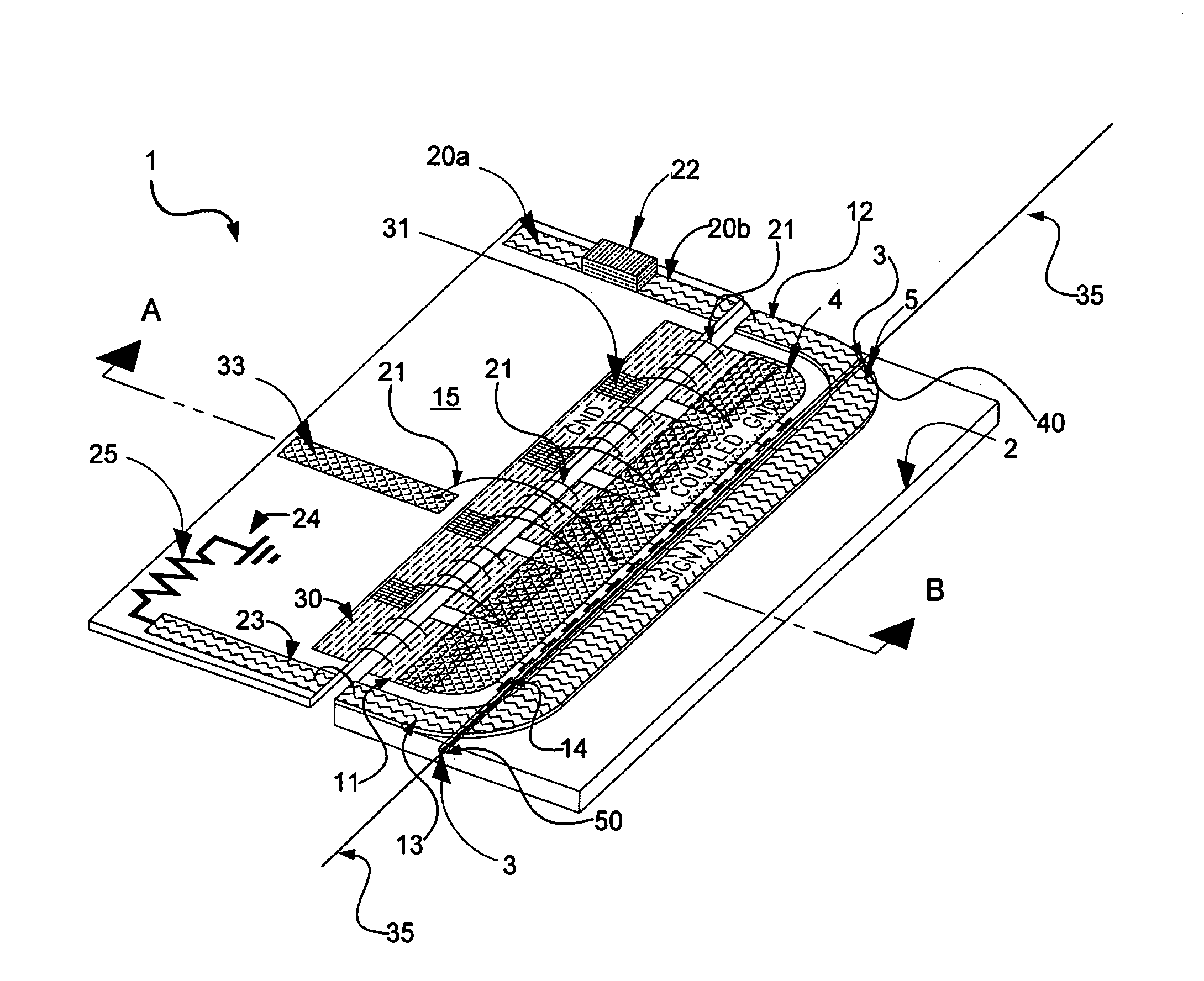
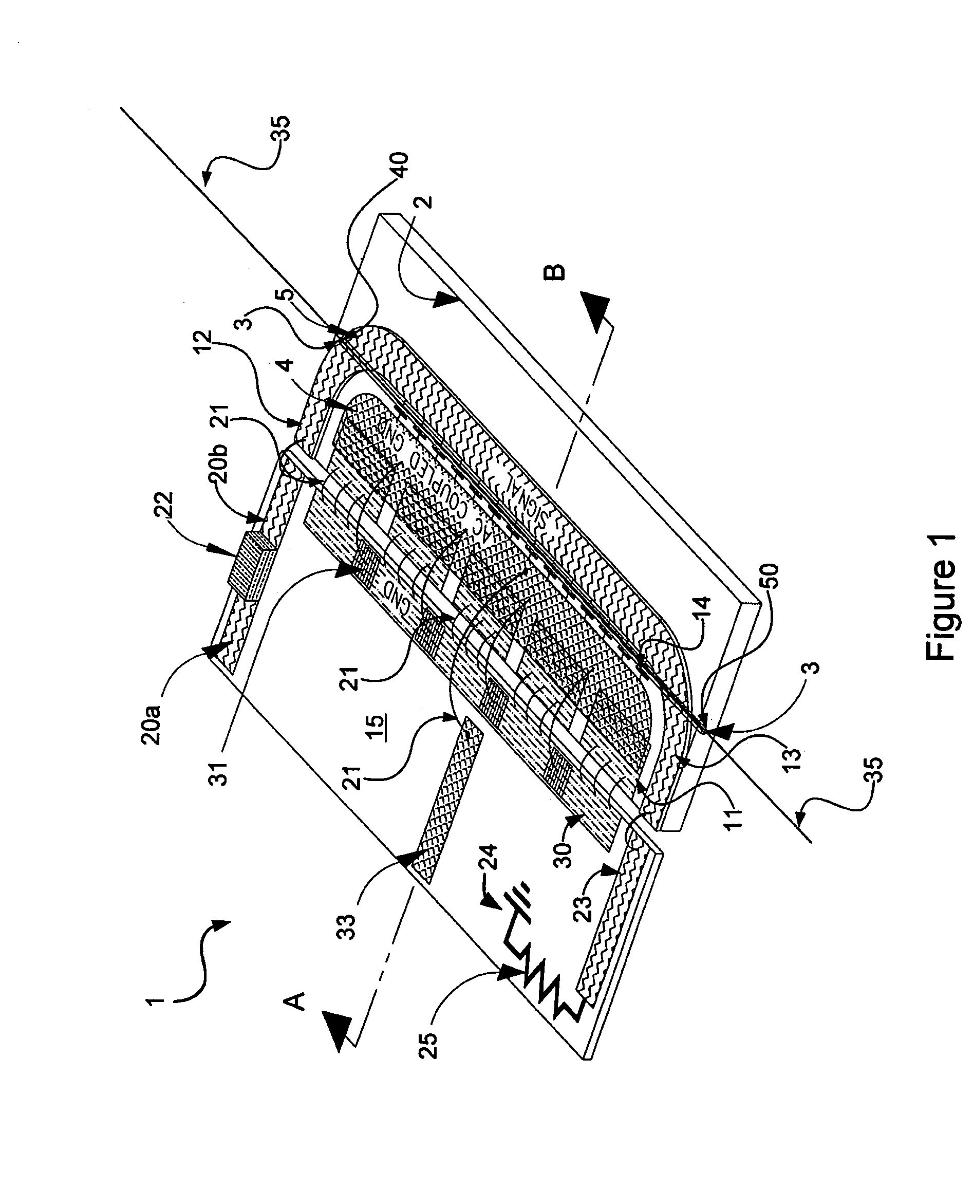
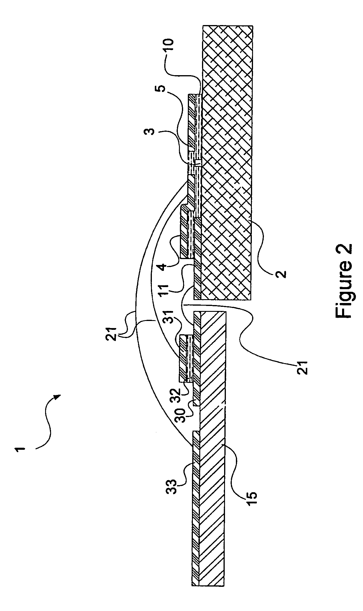
[0025]Generally, the present invention provides a system for extending the operational bandwidth of an opto-electronic polarization modulator.

[0026]In the system of the present invention, an electrical signal path is used as an electrode, as is an AC coupled ground. As an electrical signal is applied to the electrical signal path, an electric field is generated between the electrodes. This electric field is used to modulate the polarization state of light input to the modulator. The AC coupled ground allows for the application of a DC biasing voltage, which allows easy selection of an operating point of the circuit. The AC coupling is achieved by capacitively coupling a DC biased plate to a ground plate. The physical connection can be a series of ground plates, on the same chip, or to a single ground plate, with a dielectric disposed between the two. This creates a distributed capacitance between the two plates, which appears substantially as a short circuit over the operational ban...


PUM

PropertyMeasurementUnit
frequenciesaaaaaaaaaa
frequency responseaaaaaaaaaa
frequencyaaaaaaaaaa

Abstract

A semiconductor based electro-optic modulator comprising a capacitively coupled ground allowing for DC biasing of the modulator and a pre-distortion circuit for alleviating RF skin effect and for increasing bandwidth of modulator. Electrical components and functions of modulator partly located on an alumina pane. Reduction of thermally-induced stresses by connecting modulator ground to package ground via alumina pane is also disclosed.

Description

FIELD OF THE INVENTION[0001]The present invention relates generally to electro-optic modulators. More particularly, the present invention relates to electro-optic modulators having extended bandwidths.BACKGROUND OF THE INVENTION[0002]Electro-optic modulators are used in optical communications systems to rapidly modulate and optical signal in accordance with an electrical signal. In an electro-optic mode converter, a type of electro-optic modulator, an input beam of light having an input state of polarization (SOP) impinges on and traverses through an electro-optic waveguide that is subjected to an applied electric field. The applied electric field modifies the modal properties of the waveguide via the electro-optic effect. When the input SOP is not aligned with a principal axis of the waveguide, and the propagation speed of the light through the two principle axes differs, the beam of light at the output of the waveguide will generally have an output SOP different from the input one...

Claims


Application Information

Patent Timeline
Patent Type & Authority Patents(United States)
IPC IPC(8): G02F1/035G02B6/00
CPCG02F1/0356G02F2203/20
Inventor BULL, JEFFREY D.FAIRBURN, MARKJAEGER, NICOLAS AUGUST FLEMING
Owner OPTELIAN ACCESS NETWORKS
Why Eureka
Try Eureka