Manufacturing method of optical devices

a manufacturing method and optical wafer technology, applied in the direction of manufacturing tools, camera filters, instruments, etc., can solve the problems of poor utilization efficiency of optical materials, difficult to split optical wafers, and high material costs, so as to suppress processing distortion, suppress processing distortion of optical wafers, and reduce material costs

Inactive Publication Date: 2007-01-23
NIHON DEMPA KOGYO CO LTD
View PDF6 Cites 3 Cited by
  • Summary
  • Abstract
  • Description
  • Claims
  • Application Information

AI Technical Summary

Benefits of technology

[0012]A first objective of the present invention is to provide a more productive method of manufacturing optical devices that minimizes processing distortion, maintains optical characteristics satisfactorily, and promotes smallness. A second objective of the present invention is to provide a method of manufacturing optical devices that prevents the generation of fine dust and maintains the optical characteristics satisfactorily. A third objective of the present invention is to provide a method of manufacturing optical devices of a multi-layer configuration that are obtained by applying a scribing / cutting method.
[0014]Since this configuration is a scribing / cutting method in which pressure is applied to hairline cracks formed by a diamond blade edge on the optical wafer, to split it, there is no frictional resistance generated in the divided surfaces as there is in prior-art cutting methods (such as those using dicing saws), making it possible to suppress processing distortion. Note that the scribing / cutting method has advantages concerning losses of the workpiece due to the blade edge and its processing speed, and it has been specifically discovered that processing distortion of the optical wafer is suppressed by the present invention.
[0015]Thus the transmitted wave front precision in the outer peripheral areas of each of the optical devices that are divided from the optical wafer 1A is satisfactory, ensuring the optical characteristics thereof. In addition, since the entire surface of each optical device is the effective area thereof, the device can be made smaller. Furthermore, since there are no wasteful shavings from the cut surfaces due to the dicing saw, an especially large number of devices can be produced from the optical wafer, improving productivity.

Problems solved by technology

Since this means that wasteful shavings portions are generated from the multi-layer optical wafer 4, the utilization efficiency of the optical material is bad.
If the optical material is crystal, in particular, the material costs also pile up, which is wasteful.
If this scribing / cutting method is applied to the multi-layer optical wafer 4 (see FIG. 7B) formed of the three optical wafers 1A, 1B, and 1C, however, a problem arises in that it is difficult to split the optical wafer after the hairline cracks (scribed grooves) 5 have been provided, due to the adhesion of the adhesive 3 interposed between the multiple surfaces of the multi-layer optical wafer 4.
This leads to a problem in that the optical characteristics are adversely affected by the deposition of fine dust on the main surfaces of the optical device after the splitting of the optical wafer.
Thus there are stress concentrations in the vicinity of the processed layers that at the positions of the cuts, due to frictional resistance, causing distortion (processing distortion).
This processing distortion remains unchanged on the outer peripheral edges of each optical filter after the optical wafer has been divided, reducing the transmitted wave front precision in those areas and ultimately causing deterioration of the optical characteristics.
This impedes any effort to make the optical device smaller and also causes an inevitable problem concerning productivity, especially when making the multi-layer optical wafer 4 even smaller.
This not only affects these multi-layer optical wafers 4; similar problems occur when forming an optical filter from a single sheet (a single chip) or forming wavelength plates other than optical filters.

Method used


Image

  • Manufacturing method of optical devices
  • Manufacturing method of optical devices
  • Manufacturing method of optical devices

Examples


embodiments

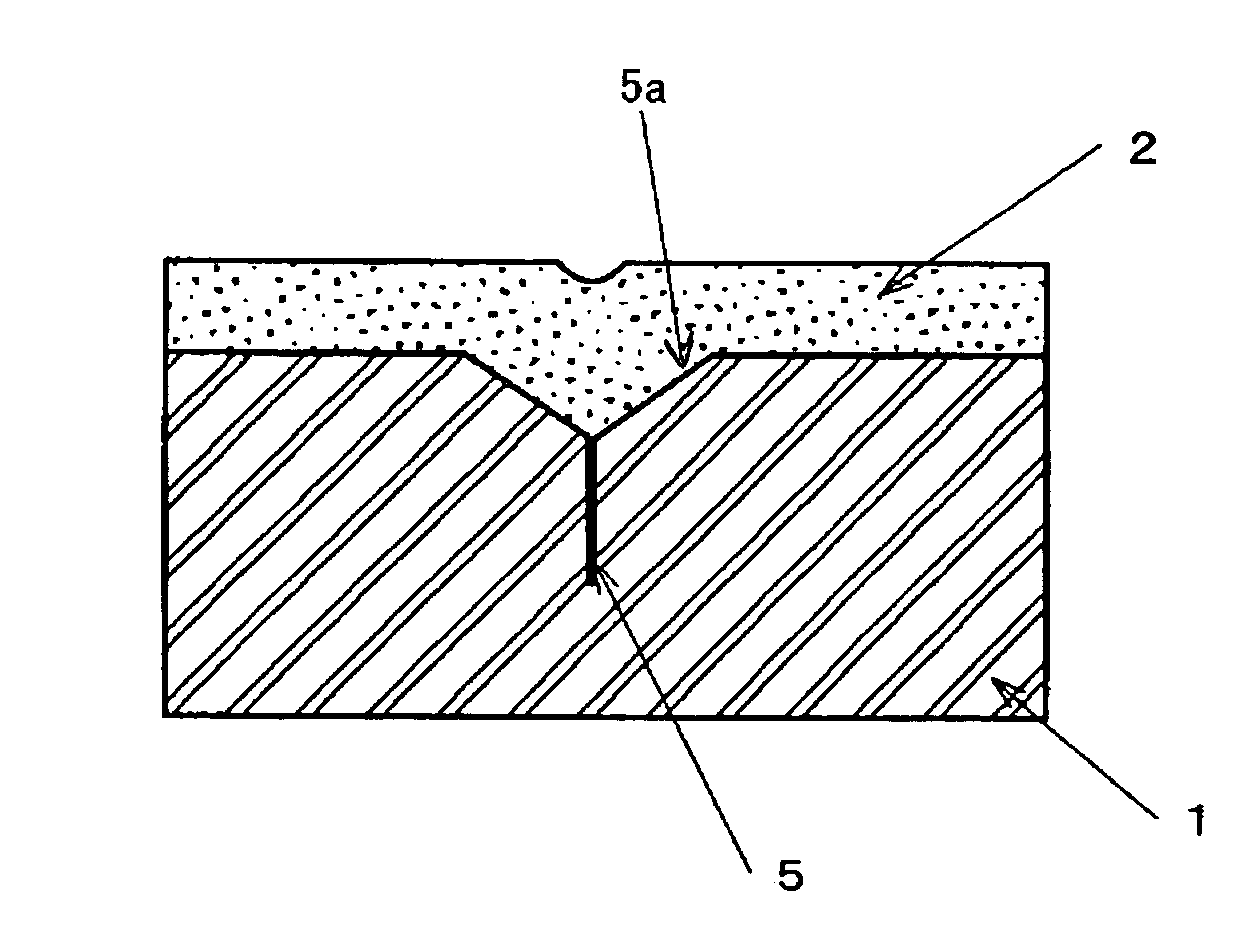
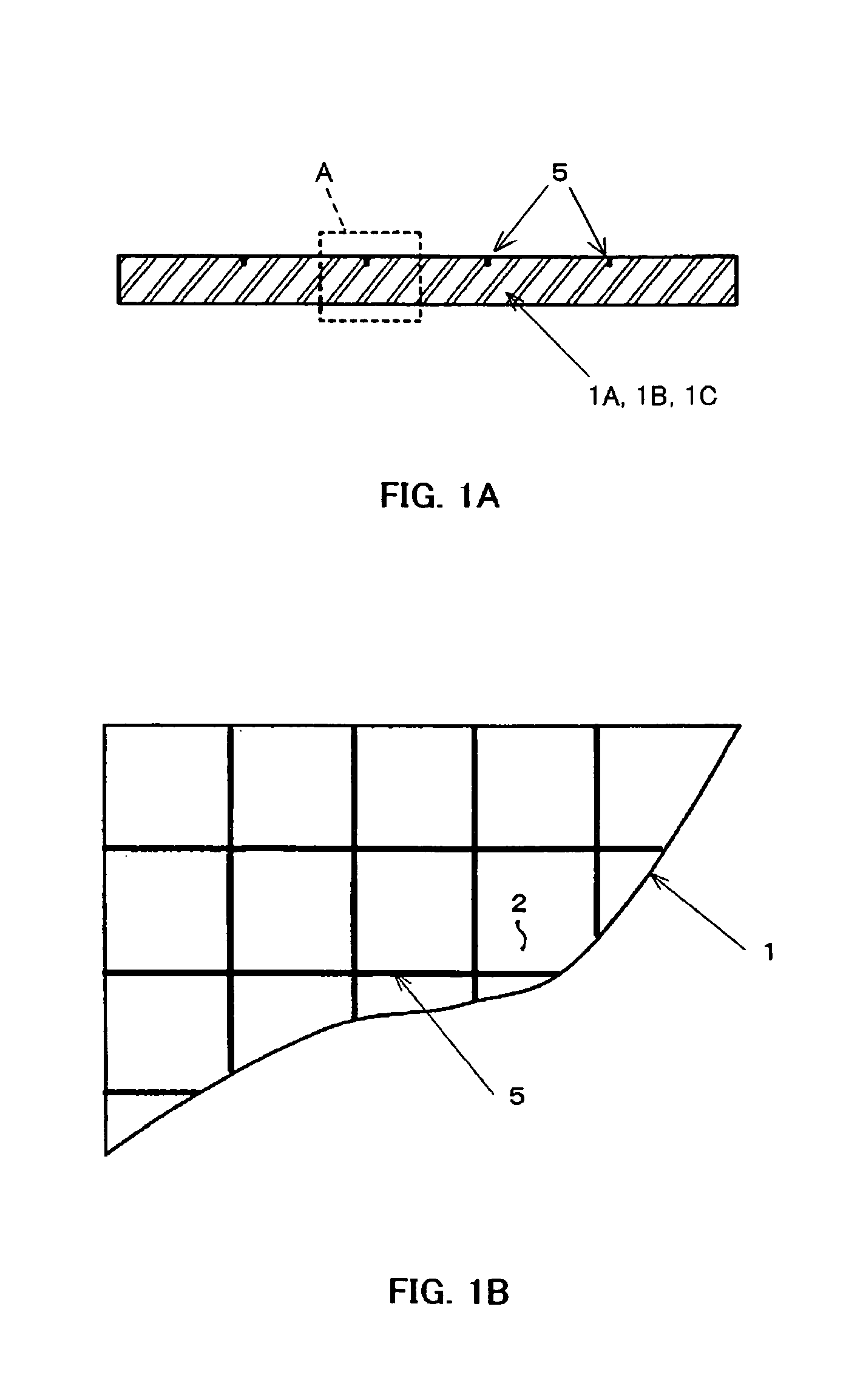
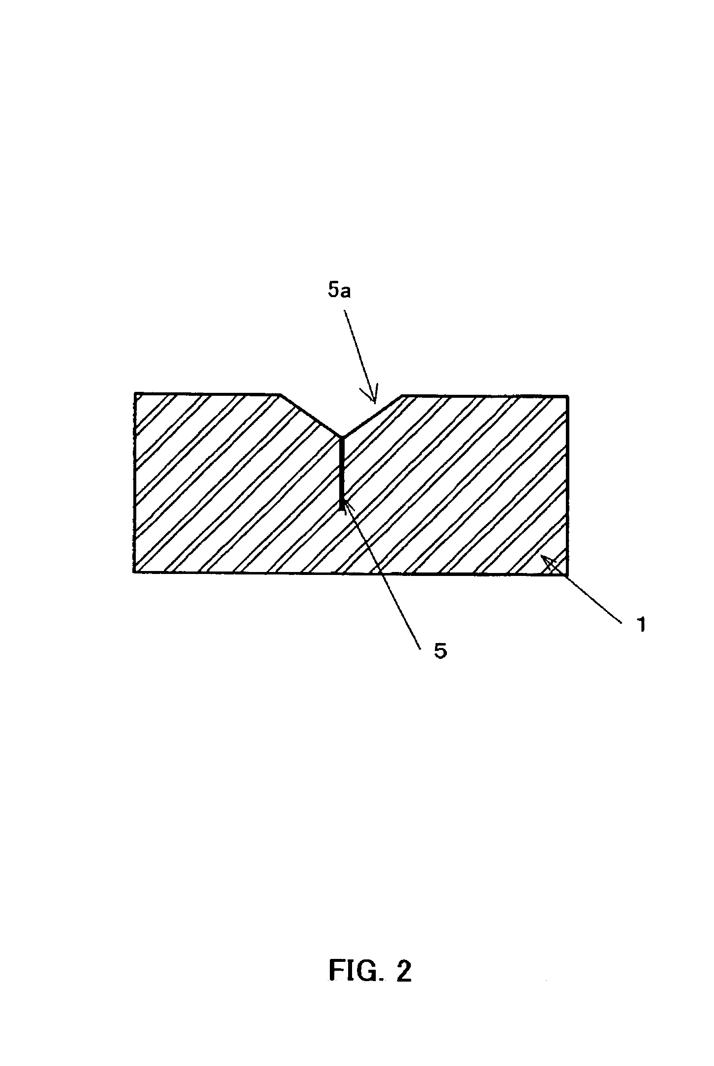
[0028]A method of manufacturing an optical device (filter) in accordance with the present invention is shown in FIGS. 1A to 3, where FIG. 1A is a vertical section through an optical wafer, FIG. 1B is a plan view thereof, FIG. 2 is a partial expanded plan view of the portion within the dotted frame A in FIG. 1A, FIG. 3A is a vertical section through an optical wafer provided with an optical thin film, and FIG. 3B is a partial expanded view of the portion within the dotted frame B in FIG. 3A.

[0029]With this invention, the optical filter is formed of multiple layers of the three optical chips 1a, 1b, and 1c, each formed of an optical material with the infrared-cutting optical thin film 2 on both main surfaces thereof, as described above, bonded together by the adhesive 3 (see FIG. 5). With the present invention, the optical chip is basically formed by first, second, and third steps.

[0030]In the first step, hairline cracks (scribed grooves or scratched grooves) 5, which define the optic...


PUM

PropertyMeasurementUnit
pressureaaaaaaaaaa
chromatic aberrationaaaaaaaaaa
widthaaaaaaaaaa

Abstract

A first objective of the present invention is to provide a more productive method of manufacturing optical devices that minimizes processing distortion, maintains optical characteristics satisfactorily, and promotes smallness. A second objective thereof is to provide a method of manufacturing optical devices that prevents the occurrence of fine dust and maintains the optical characteristics satisfactorily. A third objective thereof is to provide a method of manufacturing optical devices of a multi-layer configuration that are obtained by applying a scribing / cutting method. A method of manufacturing optical devices in accordance with the present invention, wherein an optical wafer having surfaces polished to a mirror finish is divided into a plurality of optical chips, is provided with a first step of providing hairline cracks by a diamond blade edge in one main surface of the optical wafer and a third step of applying pressure along the hairline cracks after the first step, to divide the optical wafer into the plurality of optical chips.

Description

BACKGROUND OF THE INVENTION[0001]The present invention relates to a method of manufacturing optical devices such as an optical low-pass filter (hereinafter called an “optical filter”) and, in particular, to a method of manufacturing an optical filter in which high quality is maintained.[0002]An optical filter is known in the art as a device that is disposed in front of an imaging device such as a camera, to suppress spurious signals and eliminate problems such as chromatic aberration. As the numbers of optical products have increased recently, and also the demands thereon have become more varied, the requirement is for reliable maintenance of the optical characteristics thereof, such as a high transmitted wave front precision.[0003]A method of manufacturing an optical filter in accordance with the prior art is shown in FIGS. 6 to 7C, where FIG. 6 is a vertical section through an optical filter, FIG. 7A is a vertical section through an optical wafer, FIG. 7B is a vertical section thr...

Claims


Application Information

Patent Timeline
Patent Type & Authority Patents(United States)
IPC IPC(8): H01L21/00G03B11/00B05D5/06C03B33/02G02B27/46H01L21/301
CPCG02B27/46
Inventor TAKADA, MOTOOADACHI, KAZUMASA
Owner NIHON DEMPA KOGYO CO LTD
Why Eureka
Try Eureka