Al technical title is built by PatSnap Al team. It summarizes the technical point description of the patent document.
a technology of semiconductors and heat sinks, applied in the direction of dielectric characteristics, printed element electric connection formation, printed circuit aspects, etc., can solve the problems of requiring many hundreds of connections to external devices, affecting the use of chips, and presenting serious drawbacks, etc., to achieve simple distribution and assembly, good resistance to thermal stress, and not waste of extra spa
Inactive Publication Date: 2007-01-23
TESSERA INC
View PDF123 Cites 65 Cited by
Summary
Abstract
Description
Claims
Application Information
AI Technical Summary
This helps you quickly interpret patents by identifying the three key elements:
Problems solved by technology
Method used
Benefits of technology
[0018]The assembly further includes a compliant layer disposed between the subassembly of the chip and the package element and the dielectric sheet, so that the compliant layer supports the dielectric element above the subassembly. The assembly also includes vertically extensive flexible first leads embedded in the compliant layer and extending upwardly from the contacts on the chip to the central region of the dielectric element, the flexible leads being electrically connected between the chip contacts and the terminals on the dielectric element. More preferably, the package element incorporated in the assembly includes a heat sink such as a metallic, heat conductive element which also provides some physical protection to the chip as well as one or more electrical circuit elements such as capacitors. As discussed above in connection with the method, the electrical circuit elements may be connected in circuit with the chip through horizontal conductors on the dielectric element and, preferably, through second leads extending between the circuit elements and the dielectric element.
[0019]Preferred assemblies according to this aspect of the present invention provide a unitary
Problems solved by technology
For example, a complex microprocessor chip may require many hundreds of connections to external devices.
Because the speed with which a microelectronic assembly can operate is inversely related to its size, this presents a serious drawback.
They generally do not lend themselves to use with chips having contacts disposed in a so-called area array, i.e., a grid-like pattern covering all or a substantial portion of the chip front surface.
However, flip-chip assemblies suffer from significant pro
Method used
Image
Click on the blue label to locate the original text in one second.
Reading with bidirectional positioning of images and text.
Examples
Embodiment Construction
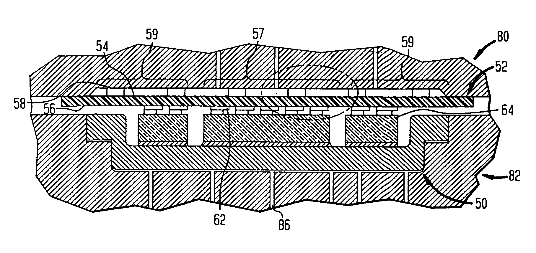
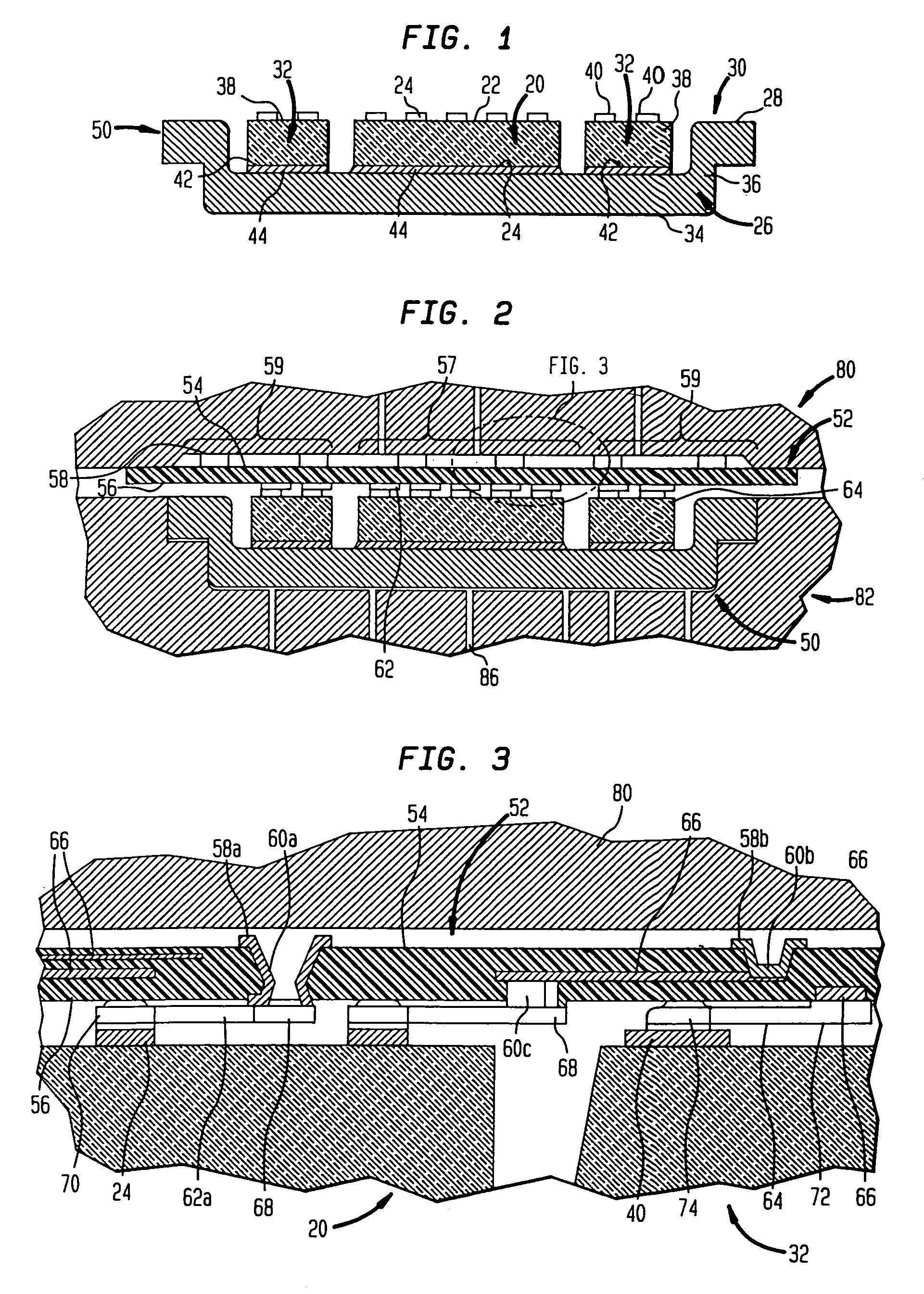
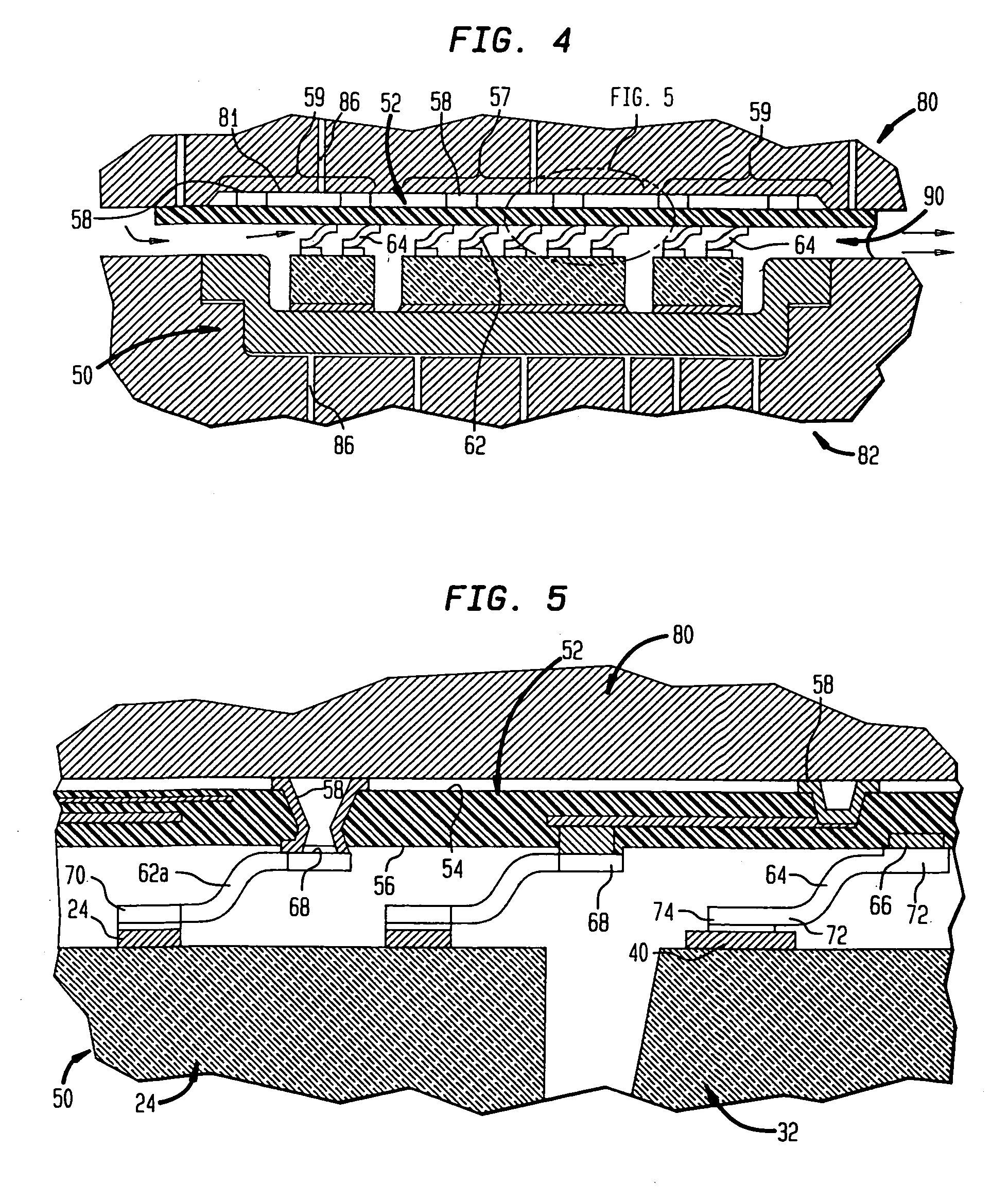
[0036]A process in accordance with one embodiment of the present invention utilizes a semiconductor chip 20 having a front surface 22 with contacts 24 thereon and having an oppositely facing rear surface24. The particular chip 20 illustrated in FIG. 1 has the contacts 24 disposed in an “area array”, i.e., an array covering substantially the entire front surface of the chip, with the contacts being uniformly spaced within the array. However, other types of chips may be used as, for example, chips having contacts disposed in rows adjacent the peripheral edges of the chip. Chip 20 is assembled with a composite package element 30 including a heat sink 26 and capacitors 32. Heat sink 26 is in the form of an open shell having a base wall 34, an edge wall 36 projecting from the base wall around the periphery thereof and a flange at the extremity of the base wall defining a generally planar flange surface 28 remote from the base wall. The auxiliary circuit elements or capacitors 32 are form...
PUM
Abstract
A packaged semiconductor chip including the chip, and a package element such as a heat sink is made by connecting flexible leads between contacts on the chip and terminals on a dielectric element such as a sheet or plate and moving the sheet or plate away from the chip, and injecting a liquid material to form a compliant layer filling the space between the package element and the dielectric element, and surrounding the leads. The dielectric element and package element extend outwardly beyond the edges of the chip, and physically protect the chip. The assembly may be handled and mounted by conventional surface mounting techniques. The assembly may include additional circuit elements such as capacitors used in conjunction with the chip.
Description
CROSS REFERENCE TO RELATED APPLICATIONS[0001]The present application is a divisional of U.S. patent application Ser. No. 09 / 863,927, filed May 23, 2001 now abandoned, which application is a continuation of U.S. patent application Ser. No. 08 / 935,962 filed Sep. 23, 1997 now U.S. Pat. No. 6,265,765, which is a divisional of U.S. patent application Ser. No. 08 / 653,016, filed May 24, 1996, now U.S. Pat. No. 5,688,716, which in turn is a continuation-in-part of U.S. patent application Ser. No. 08 / 440,665, filed May 15, 1995, now U.S. Pat. No. 5,801,441, which in turn is a divisional of U.S. patent application Ser. No. 08 / 271,768, filed Jul. 7, 1994, now U.S. Pat. No. 5,518,964.FIELD OF THE INVENTION[0002]The present invention relates to semiconductor chip assemblies and to methods and components useful in making such assemblies.BACKGROUND OF THE INVENTION[0003]Complex microelectronic devices such as modern semiconductor chips require numerous connections to other electronic components. F...
Claims
Application Information
Patent Timeline
Application Date:The date an application was filed.
Publication Date:The date a patent or application was officially published.
First Publication Date:The earliest publication date of a patent with the same application number.
Issue Date:Publication date of the patent grant document.
PCT Entry Date:The Entry date of PCT National Phase.
Estimated Expiry Date:The statutory expiry date of a patent right according to the Patent Law, and it is the longest term of protection that the patent right can achieve without the termination of the patent right due to other reasons(Term extension factor has been taken into account ).
Invalid Date:Actual expiry date is based on effective date or publication date of legal transaction data of invalid patent.