

Class-D amplifier
a class-d amplifier and amplifier technology, applied in amplifiers, amplifiers with semiconductor devices/discharge tubes, amplifiers, etc., can solve the problems of large loss, large distortion of output signals, large cost increase, etc., and achieve low distortion, small power loss, and low distortion
- Summary
- Abstract
- Description
- Claims
- Application Information
AI Technical Summary
Benefits of technology
Problems solved by technology
Method used
Image

Examples
embodiment 1
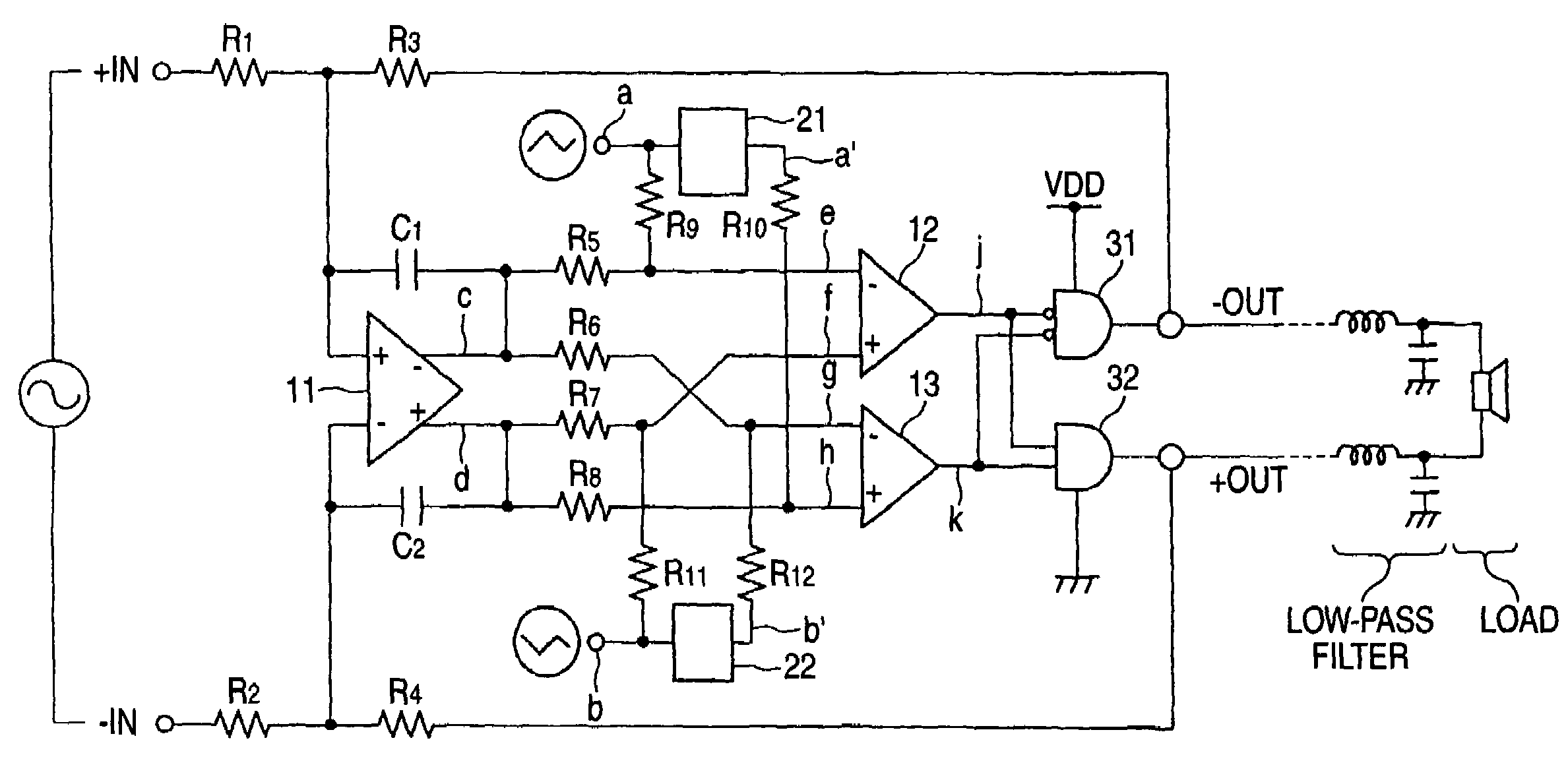
[0080]FIG. 1 is a circuit diagram for indicating a structural example of a class-D amplifier according to an embodiment 1 of the present invention.
[0081]This class-D amplifier is arranged by resistors R1, R2, R3, R4, R5, R6, R7, R8, R9, R10, R11, and R12, capacitors C1 and C2, an operational amplifier 11, comparators 12 and 13, delay circuits 21 and 22, an AND circuit (low active) 31, and another AND circuit 32. Predetermined triangular wave signals “a” and “b” are applied to one terminals of the resistors R9 and R11 respectively in this drawing. Both the triangular wave signal “a” and the triangular wave signal “b” are such signals having the same waveforms, the phases of which are different from each other by 180 degrees.
[0082]One terminals of the resistors R1 and R2 constitute differential input terminals of analog input signals, respectively. Then, one terminal of the resistor R1 constitutes a plus-sided input terminal (+IN), and one terminal of the resistor R2 constitutes a min...
embodiment 2
[0111]Next, an embodiment 2 of the present invention will now be described with reference to FIG. 5. FIG. 5 is a circuit diagram for indicating a structural example of a class-D amplifier according to the embodiment 2 of the present invention. This class-D amplifier is arranged by resistors R51, R52, R53, R54, R55, and R56, a capacitor C51, operational amplifiers 61 and 64, comparators 62 and 63, an AND circuit (low active) 71, and another AND circuit 72. A triangular wave signal “a” is applied to a plus-sided input terminal of the comparator 62, another triangular wave signal “b′” is applied to a plus-sided input terminal of the comparator 63.
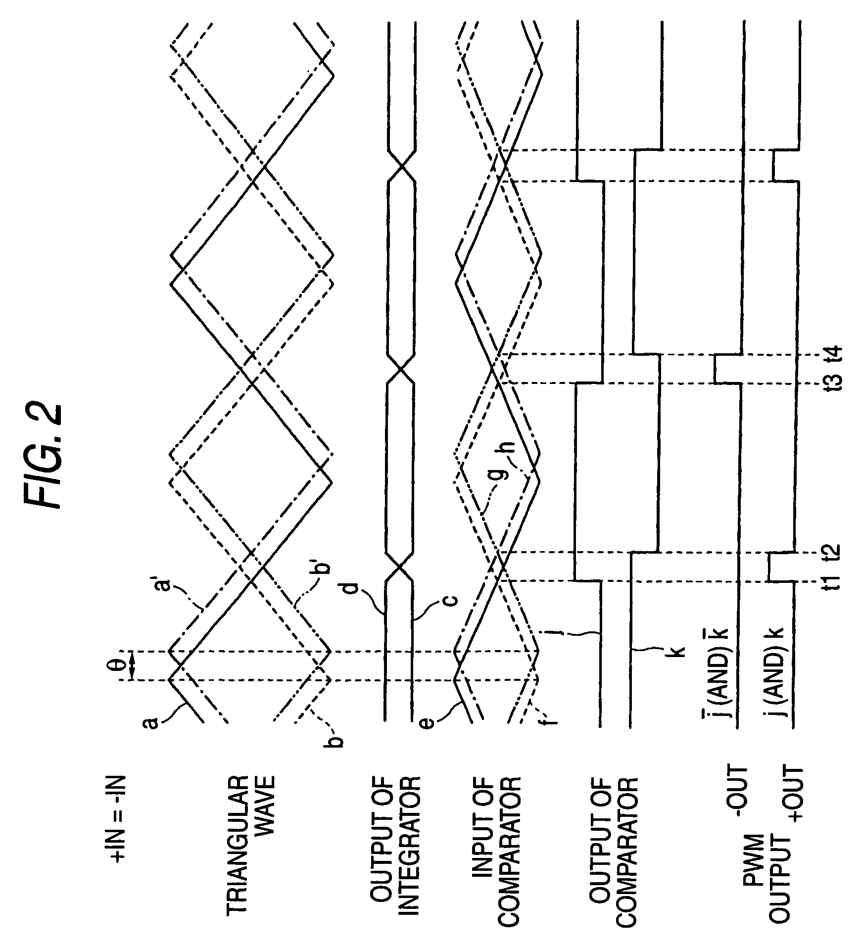
[0112]The triangular wave signal “b′” corresponds to such a triangular wave signal which is produced by that a phase of a triangular wave signal “b” obtained by inverting the triangular wave signal “a” (namely, phase is delayed by the 180 degrees) is further delayed by a very small angle “θ.” As a result, both the triangular wave signal “a” an...
embodiment 3
[0124]Next, an embodiment 3 of the present invention will now be described with reference to FIG. 8 to FIG. 11. FIG. 8 is a circuit diagram for representing a structural example of a class-D amplifier according to the embodiment 3 of the present invention. Different from the class-D amplifier according to the embodiment 1, in this class-D amplifier, the delay circuits 21 and 22 are not employed as the structural elements. In this class D amplifier, a triangular wave signal “a” is applied to one terminal of a resistor R10, whereas another triangular wave signal “b” is applied to one terminal of another resistor R12. Structural circuit arrangement other than the above-described circuit arrangement in the class-D amplifier shown in FIG. 8 are similar to those of the class-D amplifier according to the embodiment 1 shown in FIG. 1. It should be understood that respective resistance values of resistors R5, R6, R7, R8, R9, R10, R11, and R12, which constitute a synthesizing circuit in this ...
PUM
 Abstract
Description
Claims
Application Information