Method and apparatus for table and HDL based design entry

a technology of table and hdl, applied in the field of electronic circuit designs, can solve the problems of increasing complexity and decreasing the number of components on the board being designed, affecting the efficiency of modern circuit design, and increasing the size of ics, fpgas, asics, etc., and achieve the effect of convenient implementation

Inactive Publication Date: 2007-01-23
CADENCE DESIGN SYST INC
View PDF10 Cites 73 Cited by
  • Summary
  • Abstract
  • Description
  • Claims
  • Application Information

AI Technical Summary

Problems solved by technology

Modern circuit design, particularly board-level digital designs, is not as efficient as it was when schematic capture techniques were first utilized.
However, modern designs are increasing in complexity and decreasing in the number of components on the board being designed.
The increased complexity is realized in the size of the ICs, FPGAs, ASICs, and other large components now placed on the board.
Therefore, as the complexity of the component increases along with increased pin counts, there is also a corresponding increase in the complexity of the logical interconnects between the components and other components / devices on the board.
In the larger designs (e.g., a 1,000 pin FPGA) is so large that the single device will not fit on a standard sized schematic page.
Even though library tools are becoming more and more mature in their abilities to import XML, apply symbol templates and create multiple symbols, the process is not always usable for a specific device or component (particularly newly developed components).
The symbol has to be split into multiple symbols because it is too big to fit on a single schematic sheet.
Some users spend great amounts of time documenting the function of a device by annotating graphics inside the device boundary.
This is extremely time consuming and not always an effective way of describing the logical intent.
Large symbol instances leave little room for logical wiring.
This is an error-prone process and is time-consuming to capture.
However, entering connectivity in Verilog™ is also error prone as the user enters all pin names manually and then enters the signal names.
With large FPGAs or other ICs, the chances for error are significant.
Furthermore, there are difficulties for user attempting to see his / her packaging information, like reference designators and pin numbers, in the Verilog™ text file.
Adding constraints and properties is difficult, and nearly impossible in a standard text editor.
Unfortunately, the available techniques only reduce traditional design to a connect-by-name process instead of connect by logical wire.
And again, very few of the symbol's graphics indicate any logical meaning, which makes it more difficult for a designer to capture the larger picture of what the design is intended to produce.

Method used


Image

  • Method and apparatus for table and HDL based design entry
  • Method and apparatus for table and HDL based design entry
  • Method and apparatus for table and HDL based design entry

Examples


Embodiment Construction

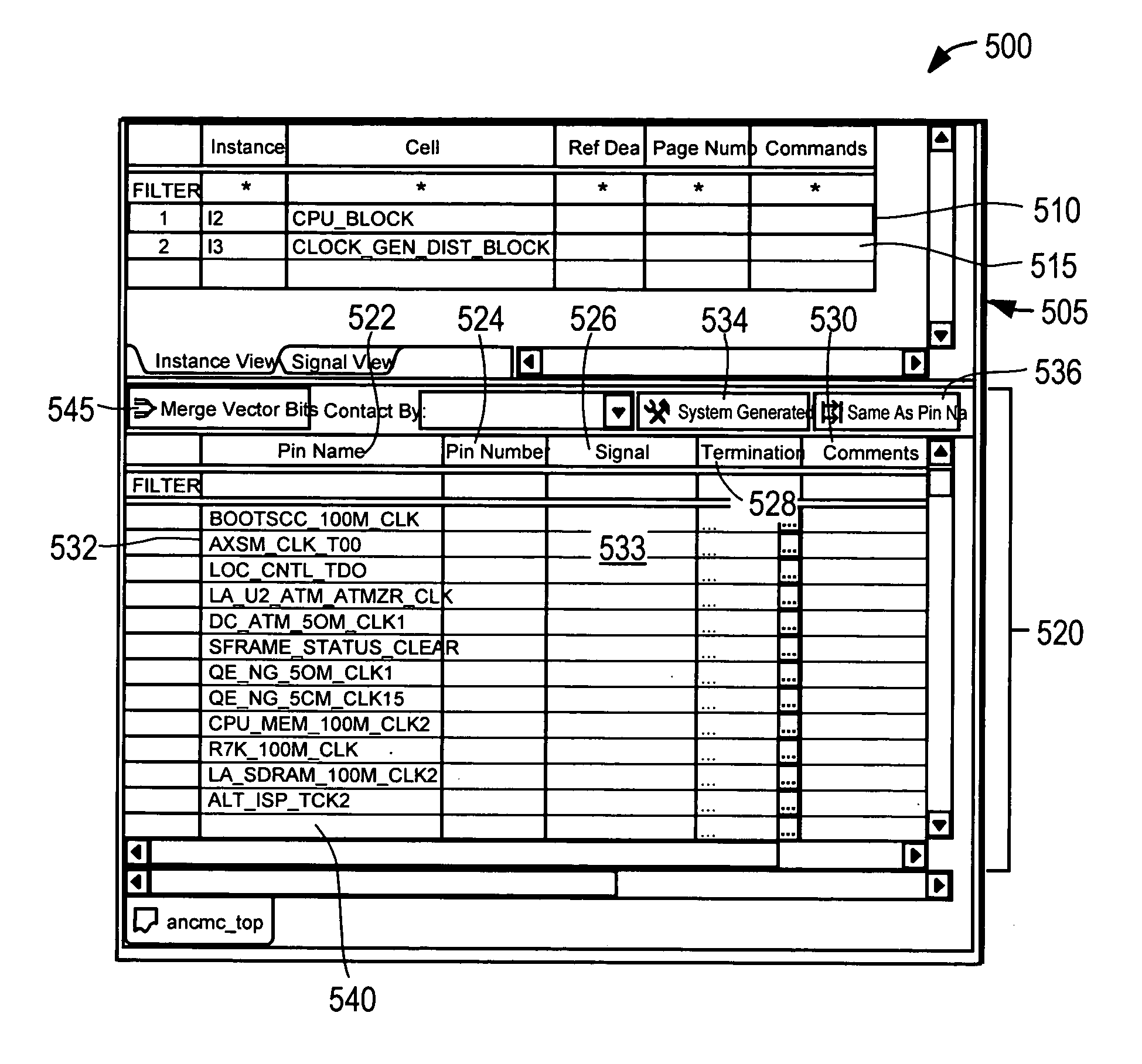
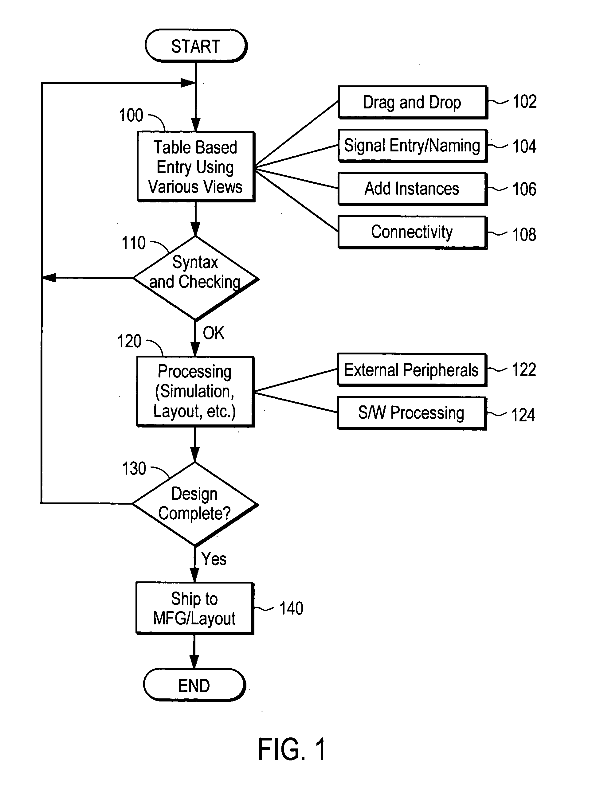
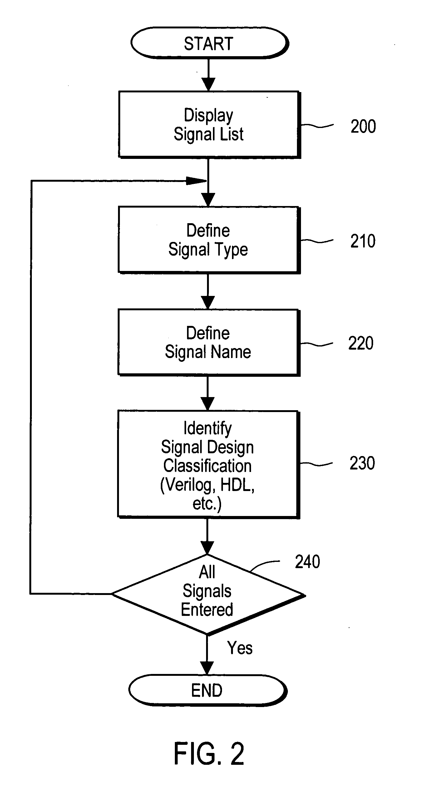
[0039]Currently, board and electronic system designers are using schematic diagrams to identify pins and signals paths (signal names) attached to the identified pins. However, as noted above, with decreased component counts and increased pin counts of modern designs, the schematic representations of a design are not very meaningful to the designer, particularly when trying to look at overall features of a design, investigate a signal path, or evaluate other features of a design. This is mainly due to the fact that large pin count component needs to be split between multiple schematic symbols (or parts of a single symbol). Once the schematic is drawn, the pins are labeled, wires are attached to each pin, and signal names are assigned to each wire. However, such a technique adds little value to the designer because nothing more than a set of pins and signal names are shown, and very little, if anything, can be deduced about the overall design or a particular signal path by viewing the...


PUM


Abstract

Views for signals and instances are provided in a table based design entry system. The signal view allows a designer to enter signals to be used in a design. The signals may be individually entered or imported from pre-defined or external packages of signals. The instance view allows the designer to enter components and to define connectivity of pins of the components to signals. The components may be entered individually or imported from predefined or external packages. An naming routines provides signal name generation and copying names of other components (e.g., pin names) to name the signals. Data entered into the table based entry system is checked for errors (duplicate names, syntax, etc.), and exported to other design tools for processes such as simulation, layout, etc.

Description

COPYRIGHT NOTICE[0001]A portion of the disclosure of this patent document contains material which is subject to copyright protection. The copyright owner has no objection to the facsimile reproduction by anyone of the patent document or the patent disclosure, as it appears in the Patent and Trademark Office patent file or records, but otherwise reserves all copyright rights whatsoever.BACKGROUND OF THE INVENTION[0002]1. Field of Invention[0003]The present invention relates to electronic circuit designs, and amongst other things to a method and apparatus for entering, saving, sharing, and displaying connections in an electronic design. The invention also relates to entry and display of connections in any type of network.[0004]The invention can also be leveraged in a large pin-count Integrated Circuit Package design where the connectivity from the die to the package is defined.[0005]2. Discussion of Background[0006]Modern circuit design, particularly board-level digital designs, is no...

Claims


Application Information

Patent Timeline
Patent Type & Authority Patents(United States)
IPC IPC(8): G06F3/14G06F17/50
CPCG06F17/5045G06F17/5022G06F30/30G06F30/33G06F30/3308G06F30/31
Inventor DURRILL, STEVEKOHLI, VIKAS
Owner CADENCE DESIGN SYST INC
Why Eureka
Try Eureka