Connector with fault tolerance

a technology of fault tolerance and connector, applied in the field of integrated circuit terminals, can solve the problems of existing connectors with built-in fault tolerance, incompatibility, and the possibility of connector defects, and achieve the effect of sufficient redundancy and greater freedom

Active Publication Date: 2007-01-30
XENOGENIC DEV LLC
View PDF5 Cites 0 Cited by
  • Summary
  • Abstract
  • Description
  • Claims
  • Application Information

AI Technical Summary

Benefits of technology

[0016]In other advantages, the connector offers variable connectivity, more specifically the possibility of switching between main and alternate connection paths, thus providing a greater degree of freedom for interconnecting discrete circuit components. Further, the specific layout of the connection paths in the connector, and in particular the possibility of having spare signal conducting members within the connector, offers sufficient redundancy to establish more secure intercommunications between, for example the cells of a semiconductor wafer or the discrete components of an integrated circuit.

Problems solved by technology

However, regardless of the level of precision with which connectors are manufactured, there always remains the possibility of connector defects, such as the short-circuiting of a pair of signal conducting members or a faulty wire.
However, existing connectors with built-in fault tolerance, including the apparatus described in U.S. Pat. No. 4,722,084, do not compensate for one of the most common fault types arising during the manufacture and use of connectors, that being a pair of fused or short-circuited signal conducting members within the connector.
Unfortunately, such a fault, if undetected, may result in improper signal connections, and thus faulty signal exchanges, between discrete circuit components.
If detected, such a fault may require the repair or replacement of a connector, which may increase the fabrication time and / or the cost associated with the manufacturing process.

Method used


Image

  • Connector with fault tolerance
  • Connector with fault tolerance
  • Connector with fault tolerance

Examples


Embodiment Construction

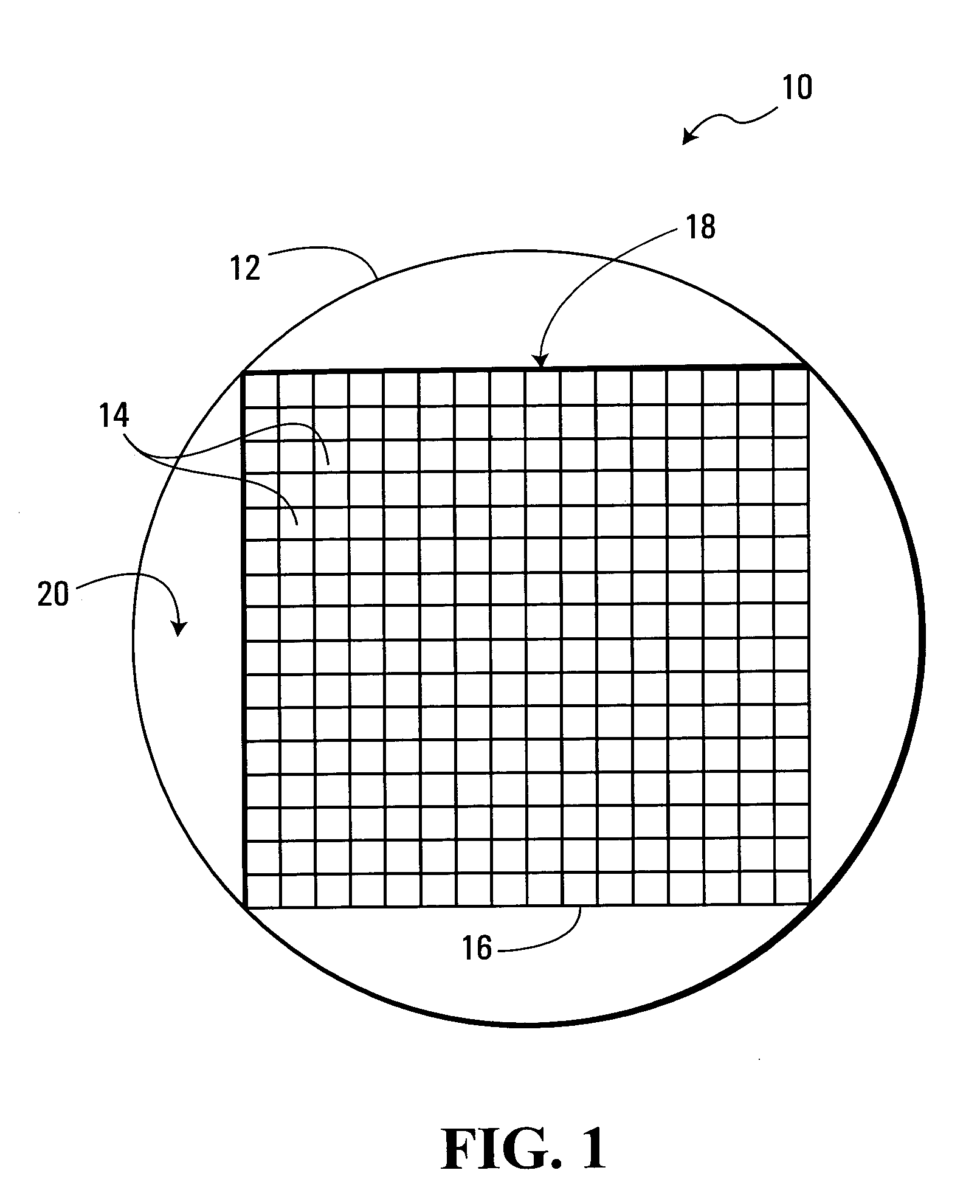
[0030]FIG. 1 is a top view of a semiconductor wafer 10, one example of a typical microelectronic complex. The wafer 10 is formed of a body of semiconductor material 12 and contains a plurality of discrete functional modules 14, also referred to as cells. In this particular example of a microelectronic complex, each discrete functional module 14 includes at least one integrated circuit.

[0031]Note that in other examples of microelectronic complexes, such as the integrated circuit itself, the discrete functional modules of the microelectronic complex include the electronic components of the integrated circuit.

[0032]The wafer body of semiconductor material 12 is made of any suitable material that has the requisite electrical properties and mechanical strength, such as silicon, germanium or gallium arsenide, and may be of any size or shape. In the example of FIG. 1, the semiconductor material of wafer body 12 is silicon, the body 12 characterized by a circular shape as a result of the cy...


PUM


Abstract

A connector including a first set of signal conducting members realized at least in part on a first surface and a second set of signal conducting members realized at least in part on a second surface, the second set being remote from the first set. In each set, the signal conducting members are arranged generally side by side. The connector also includes a plurality of connection paths, characterized by a layout for interconnecting the first and second sets of discrete signal conducting members such that signals may be exchanged between signal conducting members of the first and second sets. Specific to the invention, each signal conducting member of the first set is provided with connection paths to a different pair of non-contiguous signal conducting members of the second set.

Description

CROSS-REFERENCE TO RELATED APPLICATION[0001]The present application is based on U.S. provisional patent application No. 60 / 415,802, filed on Oct. 4, 2002, having the same inventor.FIELD OF THE INVENTION[0002]The invention relates to integrated circuit terminals, in particular to a connector with built-in fault tolerance.BACKGROUND OF THE INVENTION[0003]Microelectronic complexes, specifically systems and groups of discrete microelectronic functional modules, implement an important range of electronic devices, including microcomputers and microprocessors, and have important application in the design of electronic systems. Examples of such microelectronic complexes include semiconductor wafers containing a plurality of integrated circuits, as well as integrated circuits containing a plurality of microelectronic components.[0004]An integrated circuit typically contains multiple terminals, these being positions at which a signal connection is established or broken. Connectors are normall...

Claims


Application Information

Patent Timeline
Patent Type & Authority Patents(United States)
IPC IPC(8): G06F11/00
CPCG01R1/0491G01R31/2853
Inventor NORMAN, RICHARD
Owner XENOGENIC DEV LLC
Why Eureka
Try Eureka