Transistor circuit, display panel and electronic apparatus

a technology of transistor circuit and display panel, applied in the direction of electric variable regulation, process and machine control, instruments, etc., can solve the problems of reducing the precision of driving current, and affecting the accuracy of driving curren

Inactive Publication Date: 2007-02-06
SEIKO EPSON CORP
View PDF43 Cites 60 Cited by
  • Summary
  • Abstract
  • Description
  • Claims
  • Application Information

AI Technical Summary

Benefits of technology

[0039]According to the display panel, as input signals are provided through the compensating transistor at each picture element, the current-controlled light-emitting elements are current-controlled in response to the voltage of these input signals by the driving transistor, so that the brightness of the current-controlled light-emitting elements can be controlled with good precision without being dependent on the variance in voltage / current characteristics and threshold characteristics among the driving transistors, and that the unevenness of brightness can be reduced over the entire screen display area of the display panel. Moreover, by increasing the gate voltage of the driving transistor with the compensating transistor, the current-controlled light-emitting elements can be controlled by the input signals of a relatively low voltage.
[0041]According to such an electronic apparatus, since it has the above-described display panel, an electronic device can be realized that has little unevenness in brightness over the entire surface of the display panel and can be driven at a relatively low voltage.

Problems solved by technology

Particularly, in the case of TFTs formed in a wide range in plurality on a TFT array substrate in a display panel such as a liquid crystal panel, an EL panel, and the like, the variance in voltage / current characteristics and thresholds often becomes extremely large.
However, particularly in the case of the current-controlled element such as the EL panel mentioned above, the variance of voltage / current characteristics and thresholds tends to be a problem in the driving TFT at each picture element.
In other words, in this case, even if the voltage precision of data signals supplied to the driving TFTs from the outside is enhanced to some extent, the variance in voltage / current characteristics and thresholds in the driving TFTs appears directly as the variance of the driving current supplied to data signals, thus reducing the precision of the driving current.
Thus, this problem is, in practicality, extremely serious.
If each TFT is manufactured so as to reduce the variance in voltage / current characteristics and thresholds in consideration of this problem, the yield will decline and, particularly in the case of an apparatus with a display panel having a plurality of TFTs, the yield will decrease a great extent, and thus opposing a general goal of lower costs.
Alternatively, it is almost impossible to manufacture TFTs that can lower such a variance.
Moreover, even if a circuit for compensating the variance of voltage / current characteristics and thresholds at each TFT is installed separately, the apparatus will be complex and large, and moreover, the consumption of electric power will increase.
Particularly, in the case of a display panel wherein a plurality of TFTs are arranged at high density, the yield will decline again or it will be difficult to satisfy current demands such as lower power consumption, and miniaturization and lightening of an apparatus.

Method used


Image

  • Transistor circuit, display panel and electronic apparatus
  • Transistor circuit, display panel and electronic apparatus
  • Transistor circuit, display panel and electronic apparatus

Examples


Embodiment Construction

[0055]The operation of this invention and other benefits will be made clear by the embodiments explained below. The embodiments of this invention will be explained below with reference to the drawings.

(Transistor Circuit)

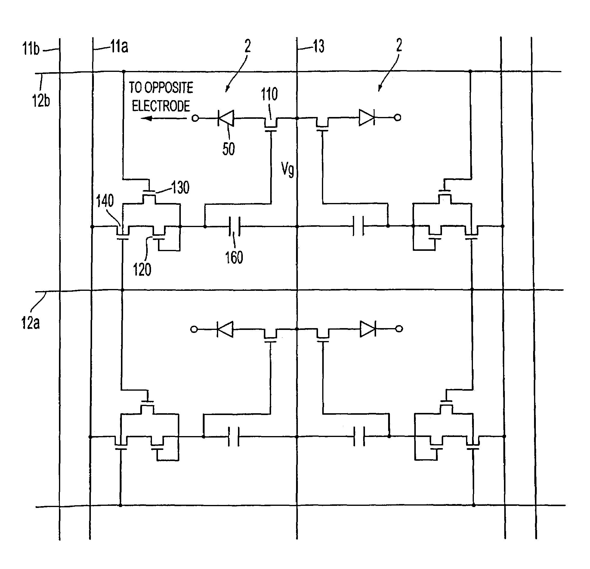
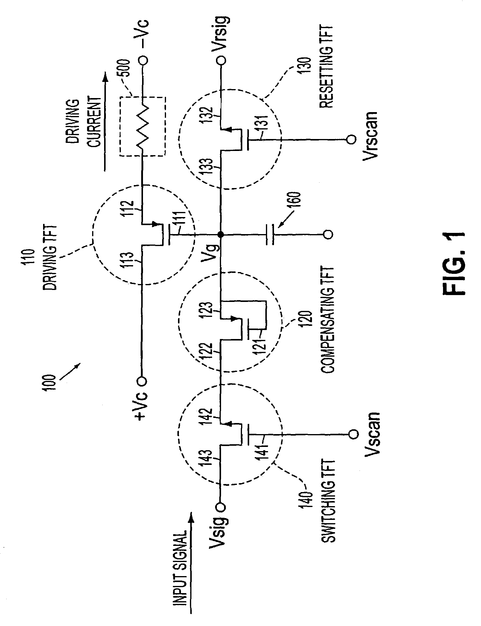
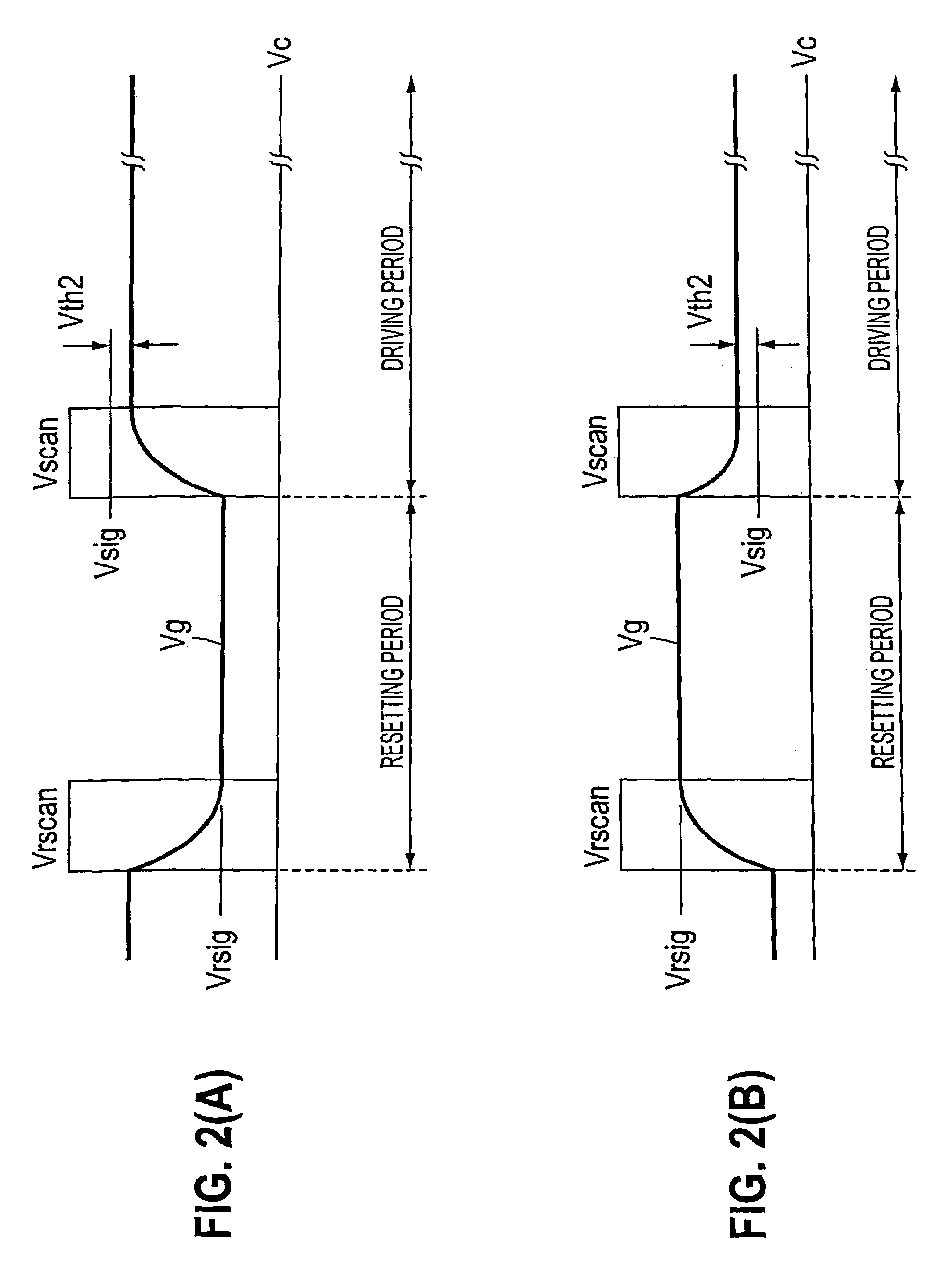
[0056]First, the embodiment of a transistor circuit of this invention is explained with reference to FIG. 1 and FIGS. 2(A)–2(B). FIG. 1 is a circuit diagram of a transistor circuit in the embodiment, and FIG. 2(A) and FIG. 2(B) are timing charts showing the timing and voltage of various signals in the transistor circuit respectively.

[0057]In FIG. 1, a transistor circuit 100 may consist of a driving TFT 110 (P channel type), a compensating TFT 120 (P channel type), a resetting TFT 130 (N channel type) and a switching TFT 140 (N channel type). The structure of each transistor will be sequentially explained below.

[0058]First, the driving TFT 110, as an example of driving transistors, is constructed so as to control conductance between a source 112 and a drain 113 in re...


PUM

PropertyMeasurementUnit
threshold voltage Vth1aaaaaaaaaa
threshold voltageaaaaaaaaaa

Abstract

A transistor circuit is provided including a driving transistor where conductance between the source and the drain is controlled in response to a supplied voltage, and a compensating transistor where the gate is connected to one of the source and the drain, the compensating transistor being connected so as to supply input signals to the gate of the driving transistor through the source and drain. In a transistor circuit where conductance control in a driving transistor is carried out in response to the voltage of input signals, it is possible to control the conductance by using input signals of a relatively low voltage and a variance in threshold characteristics of driving transistors is compensated. With this transistor circuit, a display panel that can display picture images with reduced uneven brightness is achieved.

Description

[0001]This is a Division of application Ser. No. 10 / 067,763 filed Feb. 8, 2002 now abandoned, which in turn is a division of application Ser. No. 09 / 424,043 filed Nov. 18, 1999 (and issued Mar. 26, 2002 as U.S. Pat. No. 6,362,798), which in turn is a National Stage of application No. PCT / JP99 / 01342, filed Mar. 17, 1999. The entire disclosure of the prior applications is hereby incorporated by reference herein in its entirety.BACKGROUND OF THE INVENTION[0002]1. Field of the Invention[0003]This invention relates to the technical field of transistor circuits including a plurality of transistors such as thin-film transistors (mentioned as TFT hereafter), field effect transistors and bipolar transistors, and particularly relates to the technical field of transistor circuits including driving transistors for controlling driving current, by controlling conductance between the source and the drain in response to voltage supplied to the gate, that is supplied to a driven element such as a cu...

Claims


Application Information

Patent Timeline
Patent Type & Authority Patents(United States)
IPC IPC(8): G09G3/30G05F1/00G09G3/36H05B37/02H05B39/04G02F1/136G02F1/1368G09G3/00G09G3/20G09G3/32H01L21/768H01L29/786
CPCG09G3/3233H01L21/76895G09G3/006G09G2300/0426G09G2300/0439G09G2300/0465G09G2300/0819G09G2300/0861G09G2310/0251G09G2320/043G09G2330/02G09G2330/021G09G2300/0842G09G3/30G09G3/3258G09G3/3266G09G3/3291G09G2300/0814G09G2310/0264G09G2310/061G09G2310/08G09G2320/0233
Inventor KIMURA, MUTSUMIMATSUEDA, YOJIROOZAWA, TOKUROHQUINN, MICHAEL
Owner SEIKO EPSON CORP
Why Eureka
Try Eureka