Multi-layer RF filter and balun

a filter and balun technology, applied in the field of rf signal processing circuitry, can solve the problems of difficult to match the inductance, difficult to precisely align and form the elements needed to create filter and balun devices that closely meet design requirements, and scarce board or substrate real-estate consumed by discrete components

Active Publication Date: 2007-02-13
APTIV TECH LTD
View PDF0 Cites 42 Cited by
  • Summary
  • Abstract
  • Description
  • Claims
  • Application Information

AI Technical Summary

Benefits of technology

[0012]In accordance with another aspect of the present invention, a filter for filtering a signal carried by a signal transmission line is provided. The filter is formed in a multi-layer planar substrate that includes multiple dielectric layers and multiple device layers having electrically conducting material. The filter includes symmetrical first and second inductors formed in the substrate, and also includes capacitors formed in the substrate and coupled to the inductors. A signal provided as an input to the filter is filtered by the inductors and capacitors, resulting in a filtered signal being provided at an output of the filter.
[0013]In accordance with yet another a...

Problems solved by technology

While the use of discrete baluns, filters, and combinations of baluns and filters can be effective in processing signals received by digital satellite receivers, such discrete components can consume scarce board or substrate real-estate, can be expensive, and can provide sub-optimal performance with respect to other important filter and balun characteristics noted above.
While these devices can be effective in processing signals received by digital satellite receivers, and can potentially reduce cost and board or substrate use relative to discrete components, process variation across layers and other factors can make it difficult to precisely align and form the elements needed to create filter and balun devices that closely meet design requirements.
However, because each inductor is typically formed acros...

Method used


Image

  • Multi-layer RF filter and balun
  • Multi-layer RF filter and balun
  • Multi-layer RF filter and balun

Examples


Embodiment Construction

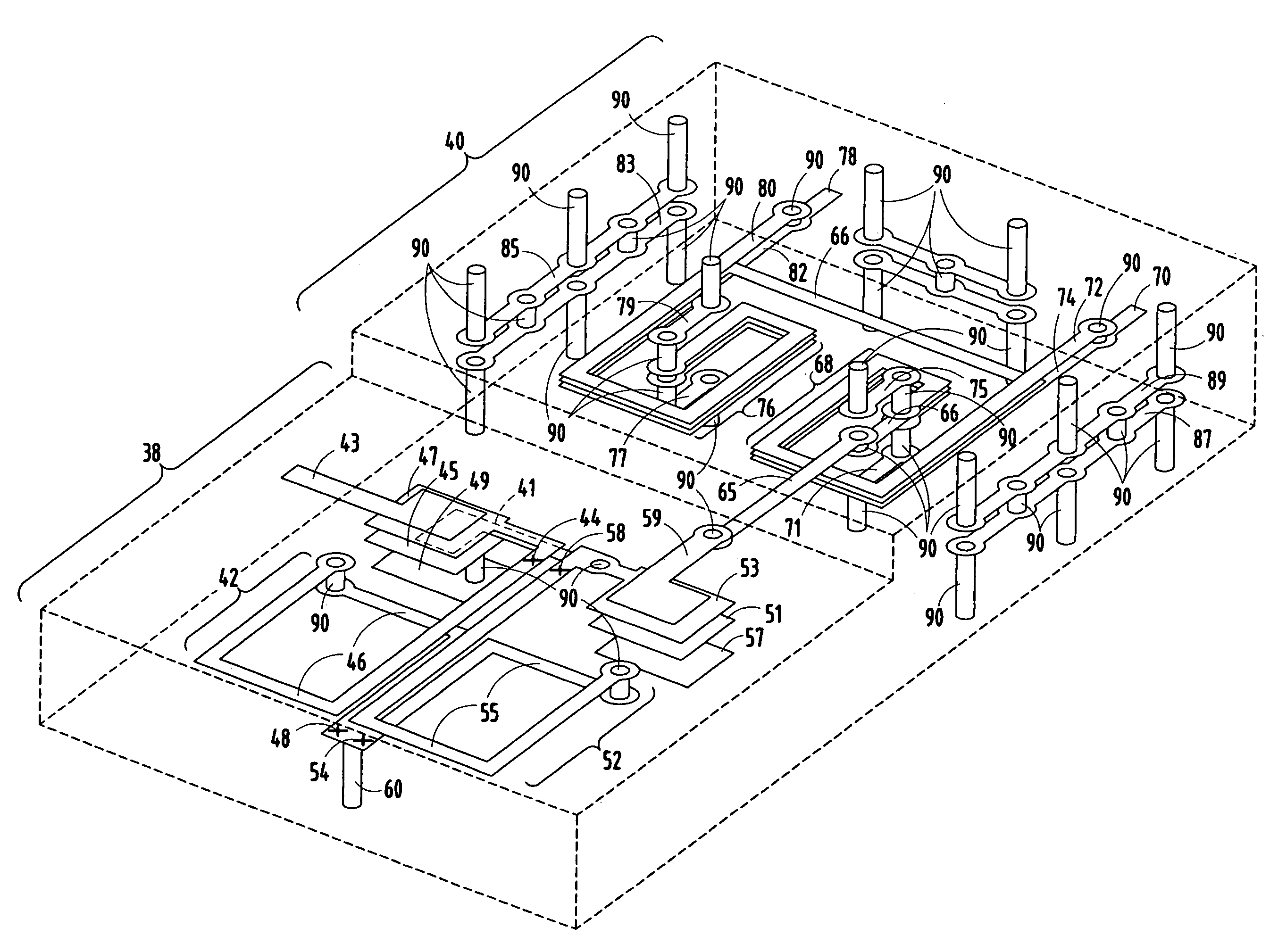
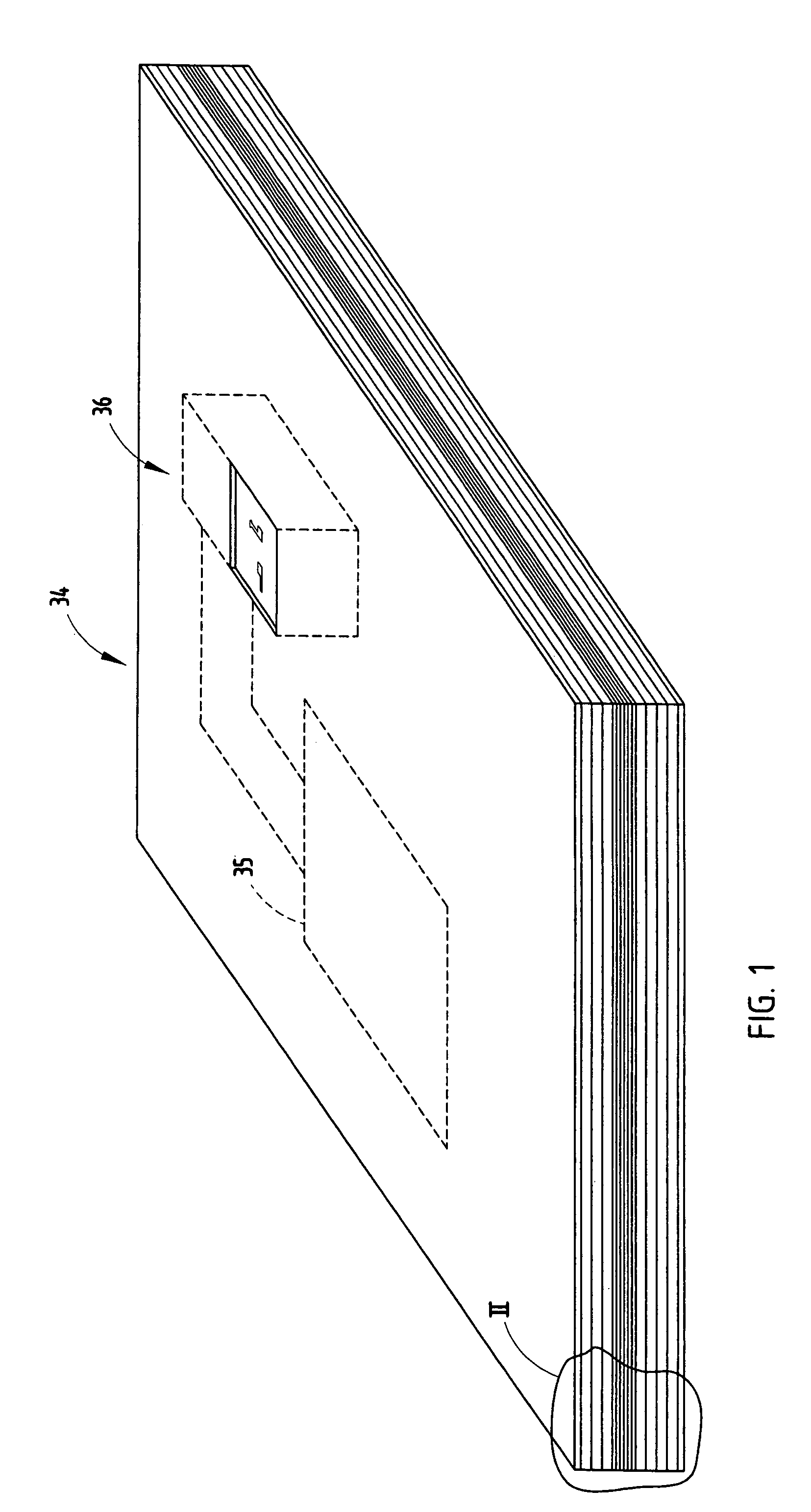
[0024]Referring to FIG. 1, a multi-layer planar substrate 34, including a filter-balun combination 36 and other electronic circuitry 35, is generally illustrated according to one embodiment of the present invention. As shown, multi-layer planar substrate 34 includes multiple planar dielectric layers and multiple planar device layers. The components forming filter-balun combination 36 are formed in the various layers of multi-layer planar substrate 34. Because most of the elements of filter-balun combination 36 are formed in the interior dielectric and device layers, they are hidden from view in FIG. 1. Multi-layer planar substrate 34 also includes electronic circuitry 35 formed in the various device layers and dielectric layers of the multi-planar substrate 34. Electronic circuitry 35 may include discrete electronic circuit elements, such as, for example, capacitors, resistors, and inductors. Electronic circuitry 35 may also include logic and memory circuitry.

[0025]According to one ...


PUM


Abstract

A filter-balun combination for filtering an RF input signal and balancing output RF signals is provided. The filter-balun combination is formed in a multi-layer planar substrate having multiple dielectric layers and multiple planar device layers having conducting material. The filter section includes first and second symmetrical inductors formed in the substrate. The inductors provide filtering for an input signal. The balun section includes a balun central transmission line connected to an output of the filter, and two output structures for providing the output from the filter-balun combination. The central transmission line follows a path through the substrate that includes first and second coil areas. The input line is sandwiched between upper and lower transmission lines in the first and second coil areas. The output of the filter-balun combination is a filtered, balanced signal at each of the two balun output structures.

Description

TECHNICAL FIELD[0001]The present invention is generally directed to RF signal processing circuitry, and, more specifically, to radio-frequency (RF) filter and balun circuitry implemented in multiple layers of a multi-layer substrate.BACKGROUND OF THE INVENTION[0002]Satellite digital audio radio services (SDARS) have become increasingly popular, offering digital radio services covering large geographic areas, such as North America. XM Satellite Radio is one example of satellite digital audio radio services. These services typically receive uplinked programming, which, in turn, is rebroadcast directly to digital radios that subscribe to the service. Each subscriber to the service generally possesses a digital radio having a receiver and antenna for receiving the digital broadcast. Although many digital radios have been designed for use in vehicles, other digital radios are increasingly being designed for use in the home or office environment, and for personal portable or wearable usag...

Claims


Application Information

Patent Timeline
IPC IPC(8): H01F5/00
CPCH01P1/2135H01P5/10H01F17/0013H05K1/165H03H2001/0085
Inventor TANTWAI, KRANTI K.DAWANDE, MANJUSHA
Owner APTIV TECH LTD
Why Eureka
Try Eureka