In-plane switching mode liquid crystal display device and method of fabricating the same

a liquid crystal display and switching mode technology, applied in static indicating devices, optics, instruments, etc., can solve the problems of narrow viewing angle, limited enhancement of viewing angle, narrow viewing angle, etc., to improve the brightness property of black color, enhance the viewing angle, and increase contrast

Inactive Publication Date: 2007-02-13
LG DISPLAY CO LTD
View PDF17 Cites 50 Cited by
  • Summary
  • Abstract
  • Description
  • Claims
  • Application Information

AI Technical Summary

Benefits of technology

[0016]An advantage of the present invention is to provide an IPS-LCD device and a method of fabricating the IPS-LCD device where brightness property of the black color is improved.
[0017]Another advantage of the present invention is to provide an IPS-LCD device is increased contrast.
[0018]Another advantage of the present invention is to provide an IPS-LCD is an enhanced viewing angle.

Problems solved by technology

However, the conventional LCD devices using the longitudinal electric field have a drawback in that they have a very narrow viewing angle.
However, since directors of liquid crystal molecules are different from each other in the IPS-LCD device including a zigzag pattern, color inversion occurs and enhancement of the viewing angle is limited.

Method used


Image

  • In-plane switching mode liquid crystal display device and method of fabricating the same
  • In-plane switching mode liquid crystal display device and method of fabricating the same
  • In-plane switching mode liquid crystal display device and method of fabricating the same

Examples


first embodiment

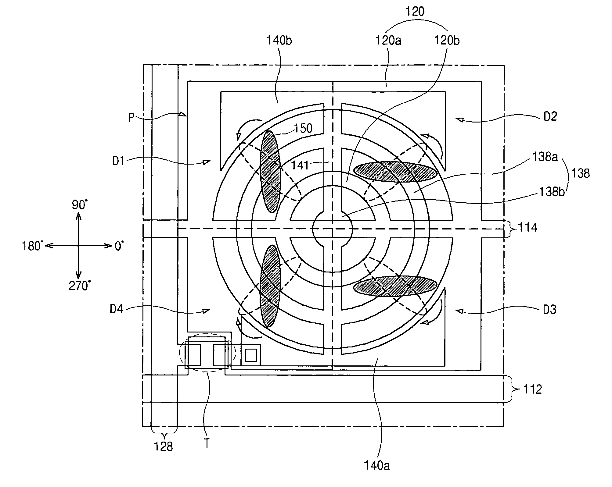
[0033]FIG. 4 is a plane view showing an IPS-LCD device according to the present invention. FIG. 4 shows one pixel region of an IPS-LCD device. A gate line 112 is transversely arranged across FIG. 4 and a data line 128 is disposed substantially perpendicular to the gate line 112. Pairs of gate and data lines 112 and 128 define a pixel region “P.” A common line 114 is parallel to and spaced apart from the gate line 112. A thin film transistor (TFT) “T” is disposed near the crossing of the gate and data lines 112 and 128. A common electrode 120 including first and second common electrode patterns 120a and 120b extends from the common line 114. A pixel electrode 138 including first and second pixel electrode patterns 138a and 138b is connected to the TFT “T.” The pixel electrode 138 alternates with the common electrode 120.

[0034]The first common electrode pattern 120a has a substantially rectangular outer side adjacent to the boundary portion of the pixel region “P” and an inner circula...

second embodiment

[0038]FIG. 5 is a plane view showing an IPS-LCD device according to the present invention. FIG. 5 shows one pixel region including four sub-pixel regions. As shown in FIG. 5, an IPS-LCD device includes red, green, blue and white sub-pixel regions “SPR,”“SPG,”“SPB” and “SPW” having a square shape. The red, green, blue and white sub-pixel regions “SPR,”“SPG,”“SPB” and “SPW” constitute one pixel region “PX.” In a high-resolution model of UXVGA having an area of 1600 mm×1200 mm, since one sub-pixel region becomes small, an orientation treatment may be performed such that liquid crystal molecules in the neighboring sub-pixel regions have alignment states to compensate retardation therebetween. For example, orientation treatment may be performed along 90° direction (or 135° direction) with respect to a direction parallel to a gate line in the red and white sub-pixel regions “SPR” and “SPW,” while the orientation treatment may be performed along 0° direction (or 45° direction) in the green...


PUM

PropertyMeasurementUnit
viewing anglesaaaaaaaaaa
brightnessaaaaaaaaaa
weightaaaaaaaaaa

Abstract

An in-plane switching mode liquid crystal display device includes: first and second substrates facing and spaced apart from each other; a gate line on the first substrate; a data line crossing the gate line to define a pixel region including a plurality of domains; a thin film transistor connected to the gate line and the data line; a common line parallel to and spaced apart from the gate line; a common electrode extending from the common line and having a ring shape; a pixel electrode connected to the thin film transistor and having a ring shape, the pixel electrode alternating with the common electrode; and a liquid crystal layer between the pixel electrode and the second substrate, the liquid crystal layer in neighboring domains having orientation directions different from each other.

Description

[0001]This application claims the benefit of Korean Patent Application No. 2003-090413, filed on Dec. 11, 2003, which is hereby incorporated by reference as if fully set forth herein.BACKGROUND OF THE INVENTION[0002]1. Field of the Invention[0003]The present invention relates to a liquid crystal display device. More particularly, it relates to an in-plane switching mode liquid crystal display (IPS-LCD) device where brightness of black color is improved.[0004]2. Discussion of the Related Art[0005]Liquid crystal display (LCD) devices are being developed as the next generation of display devices because of their characteristics of light weight, thin profile, and low power consumption. In general, an LCD device is a non-emissive display device that displays images by making use of a refractive index difference through utilizing optical anisotropy properties of a liquid crystal material interposed between an array substrate and a color filter substrate. Of the different types of known li...

Claims


Application Information

Patent Timeline
Patent Type & Authority Patents(United States)
IPC IPC(8): G02F1/1343G02F1/1337G02F1/133G02F1/136G02F1/1362G02F1/1368H01L29/786
CPCG02F1/134363G02F1/136213G02F2201/52G02F2201/122G02F2001/133757G02F1/133757G02F1/1337
Inventor LEE, YUN-BOK
Owner LG DISPLAY CO LTD
Why Eureka
Try Eureka