
Method and apparatus for reducing leakage current in a read only memory device using shortened precharge phase
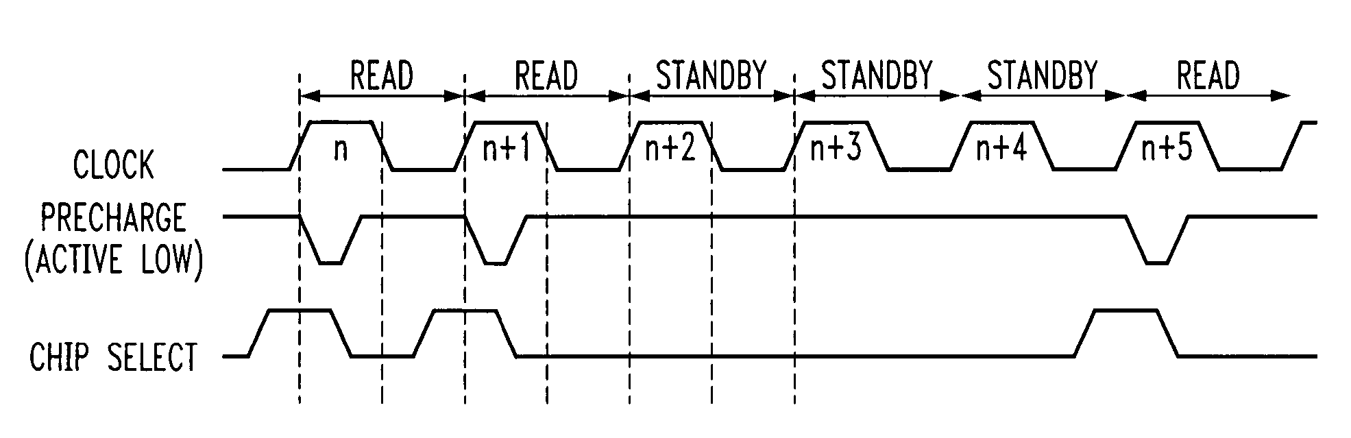
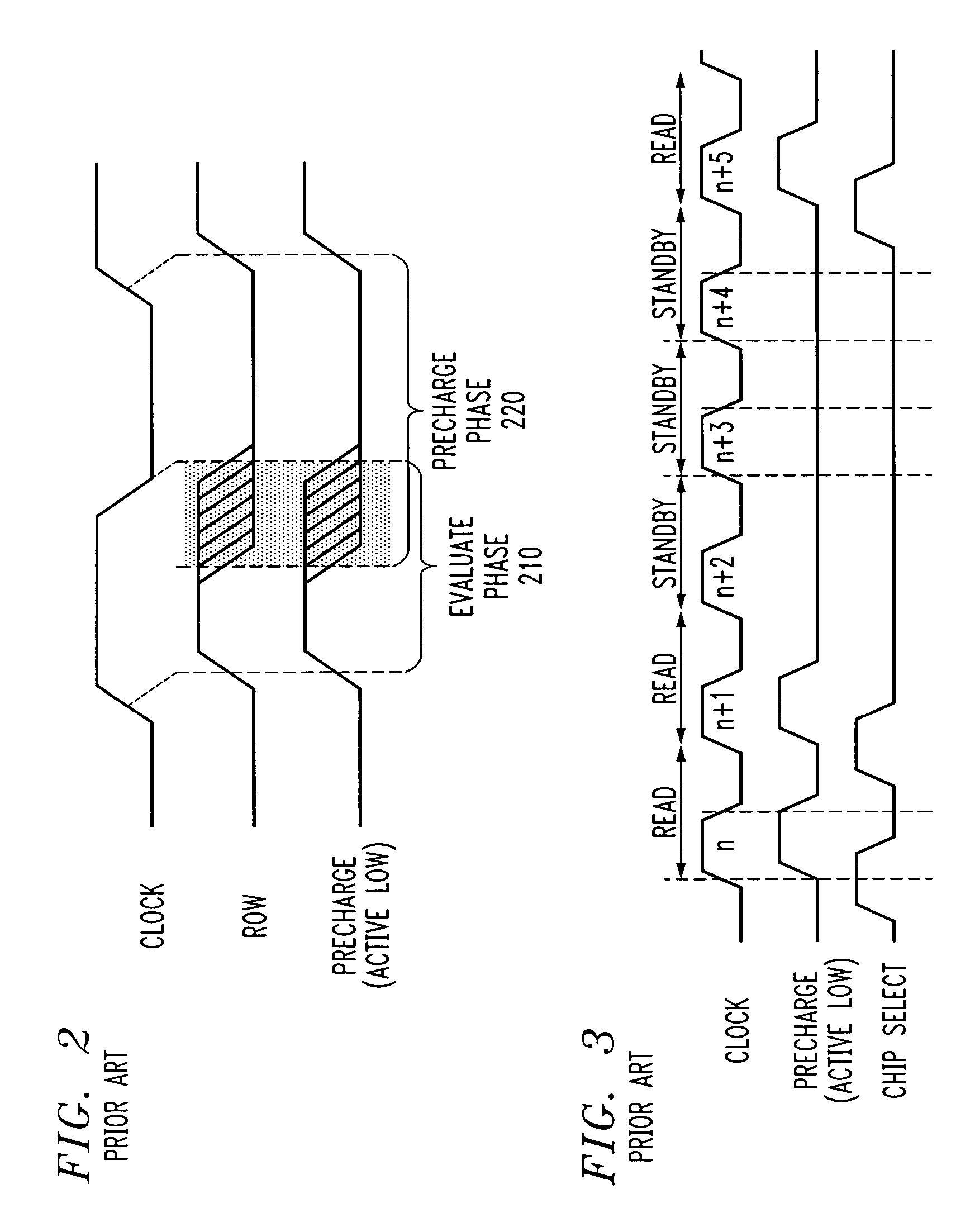
a technology of read only memory and leakage current reduction, which is applied in the field of leakage current reduction of electronic memory devices comprised of arrays of transistors, can solve the problems of high leakage current, significant problem of transistor sub-threshold leakage current, so as to reduce leakage current, reduce leakage current, and reduce the duration of the precharge cycle
- Summary
- Abstract
- Description
- Claims
- Application Information
AI Technical Summary
Benefits of technology
Problems solved by technology
Method used
Image

Examples
Embodiment Construction
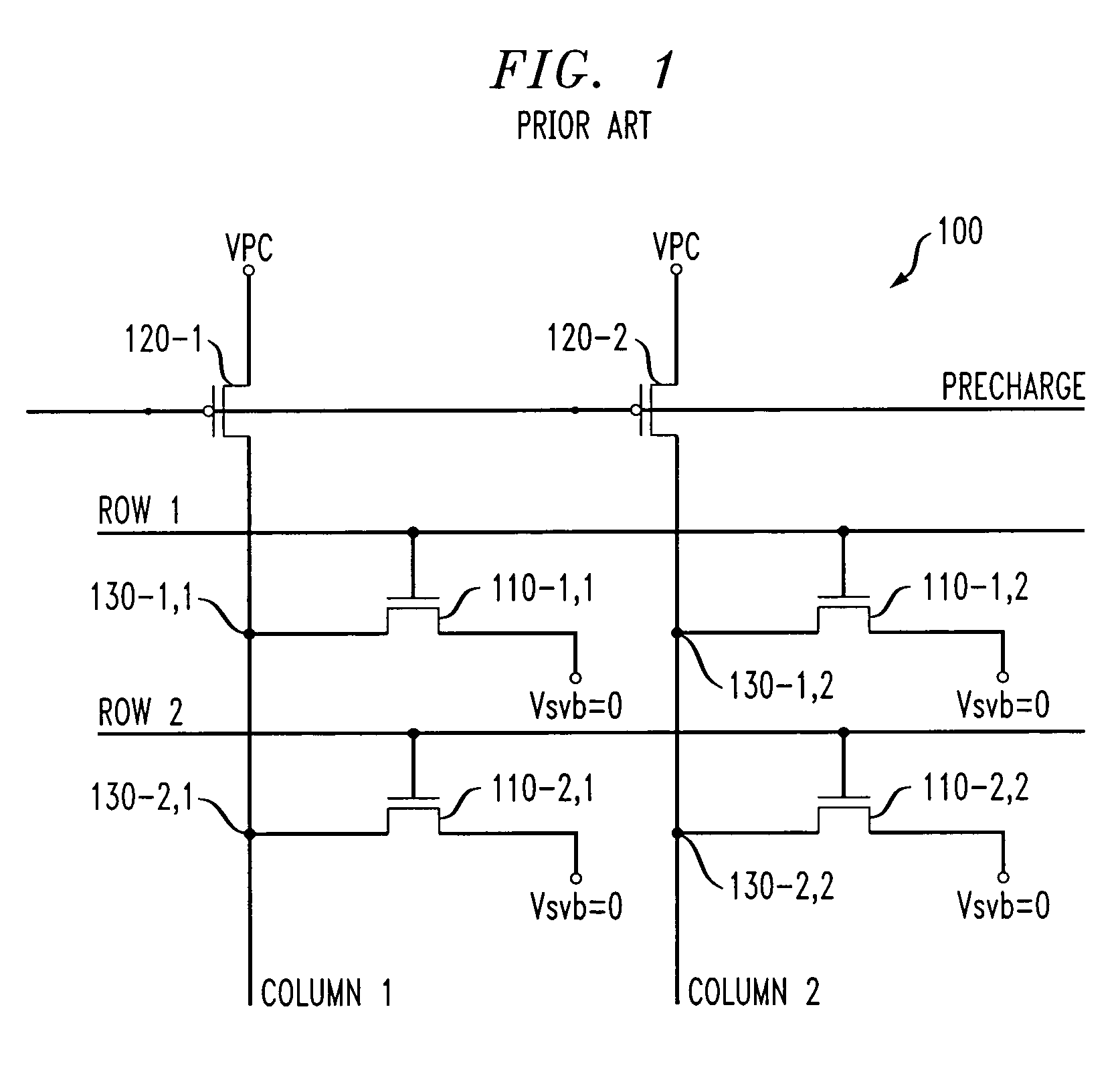
[0014]FIG. 1 illustrates a conventional ROM memory cell array with column precharge transistors that may be, for example, part of an integrated circuit. The memory cell transistors are n-channel transistors. The precharge transistors are p-channel devices. This type of ROM array is referred to as an “n-channel” array. There is also an analogous “p-channel” ROM memory array (not shown) where the cell transistors are p-channel transistors and the precharge transistors are n-channel transistors. For clarity, unless otherwise specified, all references and specified voltages here within apply to n-channel ROM memory arrays.
[0015]FIG. 1 illustrates a conventional n-channel two by two ROM array 100 of memory cells 110-1,1 through 110-i,j. The memory cells 110-1,1 through 110-i,j are generally comprised of n-channel transistors generally arranged in a grid pattern having a plurality (or series) of rows and columns. As shown in FIG. 1, the exemplary ROM array 100 includes a plurality, i, of ...
PUM
 Abstract
Description
Claims
Application Information