Method and system for inspecting electronic components mounted on printed circuit boards

a technology of electronic components and printed circuit boards, applied in the direction of material analysis, television systems, instruments, etc., can solve the problems of poor performance, false-calling of methods, and inability to directly provide lead coplanarity information,

Inactive Publication Date: 2007-02-20
ELECTRO SCI IND INC
View PDF6 Cites 15 Cited by
  • Summary
  • Abstract
  • Description
  • Claims
  • Application Information

AI Technical Summary

Problems solved by technology

These methods cannot directly provide lead coplanarity information.
These methods are subject to false-calls and poor performance (accuracy, repeatability, and robustness) due to chaos in the intensity information coming from the component leads, the solder paste deposits, and the PCB.
Inspection can also be done after reflow, but this is the most difficult point to rework and correlate.
The reflow process time between component placement and after reflow is on the order of 10–15 minutes and does not allow for real-time corrective action and process control.
Recurrent problems with placement equipment are not caught early enough to prevent production of multiple bad boards.
2-D systems do not provide height information which is necessary for coplanarity.
However, this is at the last stages of the SMT process and thus the least cost effective.

Method used


Image

  • Method and system for inspecting electronic components mounted on printed circuit boards
  • Method and system for inspecting electronic components mounted on printed circuit boards
  • Method and system for inspecting electronic components mounted on printed circuit boards

Examples


Embodiment Construction
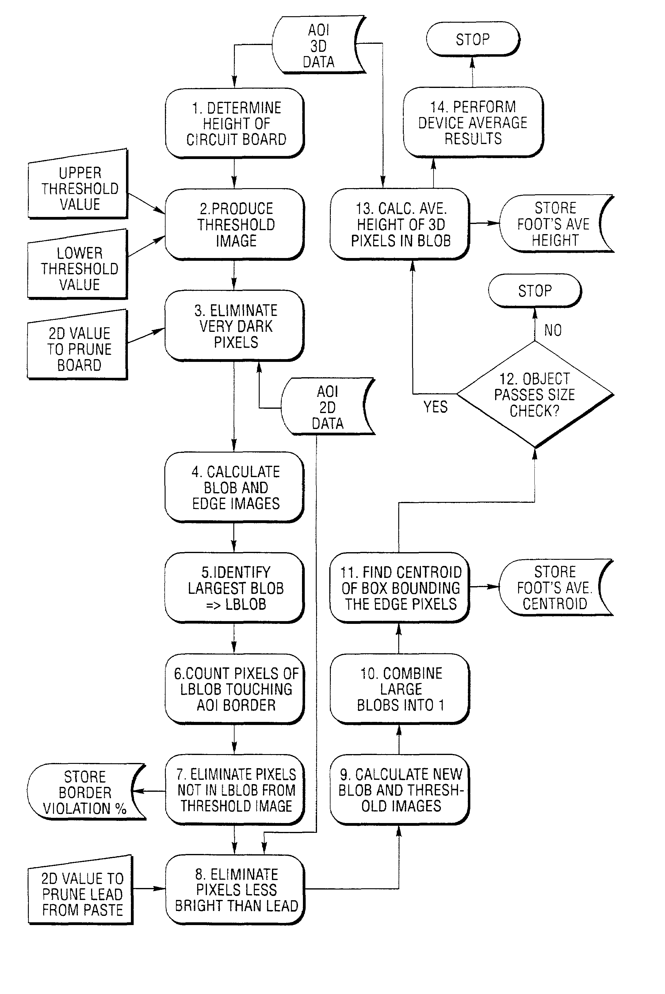
Lead Foot Algorithm

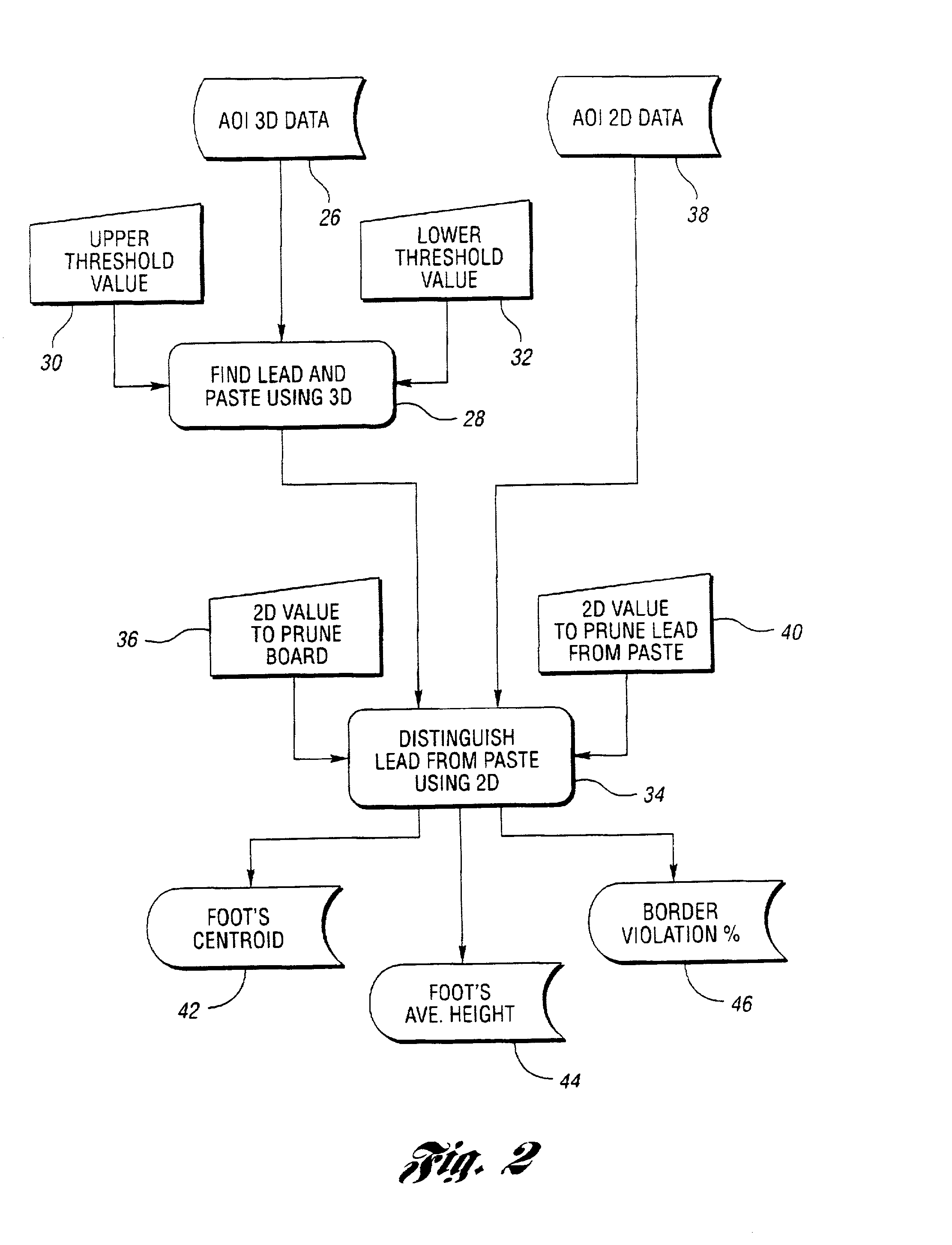
[0048]In one embodiment of the present invention, the foot of the lead is located. The method and system of the present invention rely on the fact that component leads which are difficult to identify using 2-D or 3-D data alone can be more easily identified with a combination of both 2-D and 3-D data. The following table illustrates this concept clearly:

[0049]

Visible Elements2-D Category3-D CategoryBodyDarkHighKneeBrightMedium HighFootBrightMedium LowPasteDarkMedium LowBoardDarkLowTraceBrightLow

[0050]Note that the lead (i.e., foot) cannot be uniquely identified with either the 2-D or 3-D data as categorized above, but there is a unique identity given by bright 2-D data and medium low 3-D data.

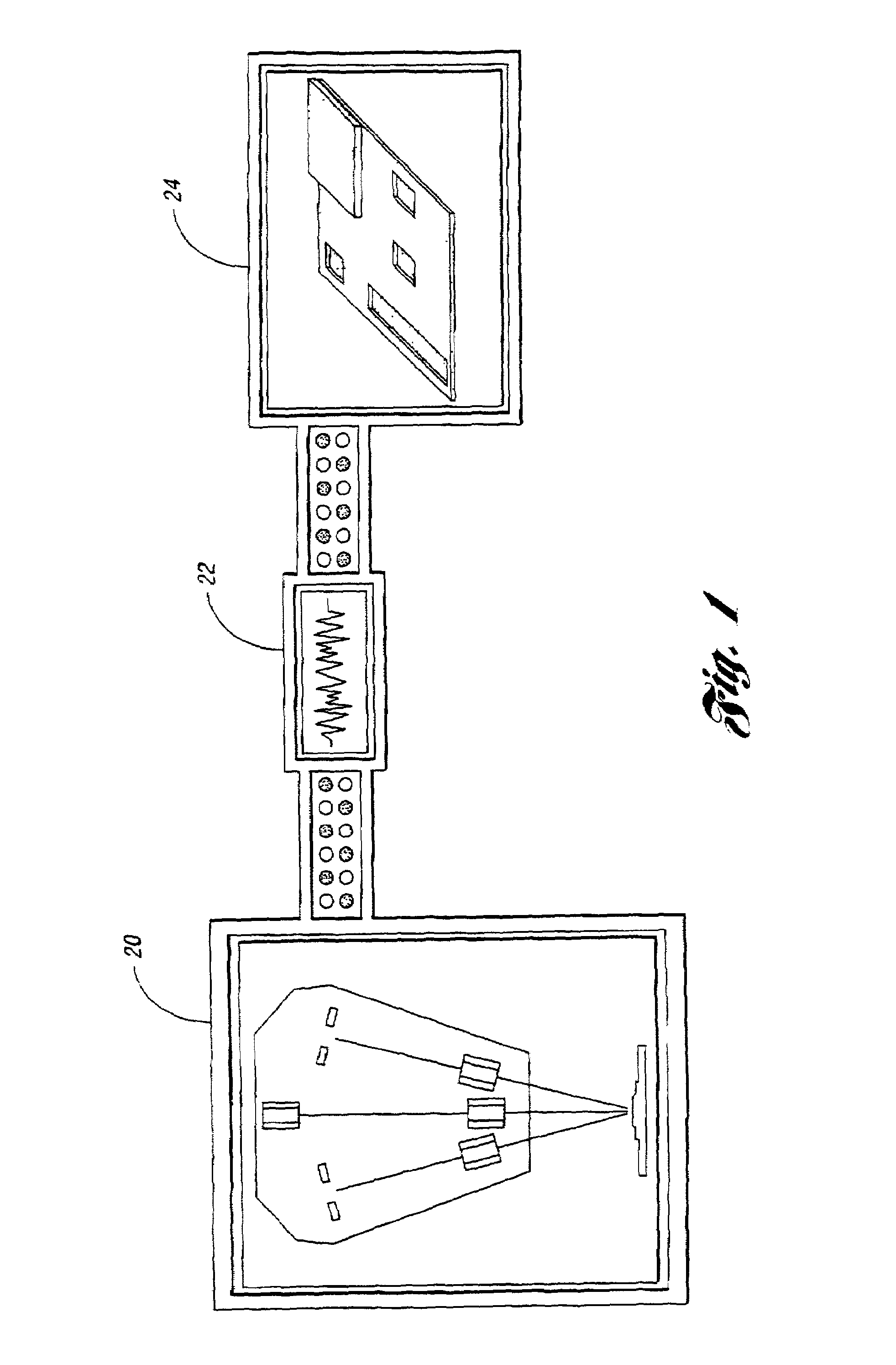
[0051]Data acquisition for the best mode is accomplished via an inspection system utilizing 3-D laser scanning technology, as illustrated in FIG. 1. At block 20, a solid state dual detector laser acquires data at millions of data points per second.

[0052]At block 22, high-spee...


PUM


Abstract

A method and system are provided for inspecting electronic components mounted on printed circuit boards utilizing both 3-D and 2-D data associated with the components and the background on which they are mounted on the printed circuit board. Preferably, a 3-D scanner in the form of a solid state dual detector laser images the components and solder paste on the printed circuit board to obtain the 3-D and 2-D data. Then, a high speed image processor processes the 3-D data to find the locations of the leads and the solder paste. Then, the high speed image processor processes the 2-D data together with the locations of the leads and the solder paste to distinguish the leads from the solder paste. The high speed image processor may calculate centroids of feet of the leads, average height of the feet and border violation percentage of the solder paste.

Description

CROSS-REFERENCE TO RELATED APPLICATION[0001]This application claims the benefit of U.S. provisional patent application Ser. No. 60 / 170,462, filed Dec. 13, 1999.TECHNICAL FIELD[0002]This invention relates to methods and systems for inspecting electronic components mounted on printed circuit boards, and is primarily intended for use at an inspection station placed in a surface mount PCB production line.BACKGROUND ART[0003]The most typical method for inspection of components including leads is with 1 2-D or intensity-only sensor, i.e., a camera of some sort. These methods cannot directly provide lead coplanarity information. These methods are subject to false-calls and poor performance (accuracy, repeatability, and robustness) due to chaos in the intensity information coming from the component leads, the solder paste deposits, and the PCB.[0004]Component placement inspection before reflow is necessary to minimize defects in the SMT process. Rework cost at this point is lower than after...

Claims


Application Information

Patent Timeline
Patent Type & Authority Patents(United States)
IPC IPC(8): G06K9/00H05K13/08
CPCH05K13/08H05K13/0817
Inventor WEISGERBER, JOHN J.SVETKOFF, DONALD J.ROHRER, DONALD K.
Owner ELECTRO SCI IND INC
Why Eureka
Try Eureka