
Non-volatile memory device and fabricating method thereof

a memory device and non-volatile technology, applied in the direction of semiconductor devices, basic electric elements, electrical apparatus, etc., can solve the problems of weak competitiveness and complicated corresponding fabrication, and achieve the effect of facilitating device fabrication, reducing cell size, and high cell integration

Inactive Publication Date: 2007-02-27
DONGBU ELECTRONICS CO LTD
View PDF3 Cites 0 Cited by
  • Summary
  • Abstract
  • Description
  • Claims
  • Application Information

AI Technical Summary

Benefits of technology

"The present invention is about a non-volatile memory device and its fabricating method. The invention aims to solve problems in the related art, such as high cell size and difficulty in fabrication. The invention provides a non-volatile memory device with a smaller cell size and easier fabrication. It includes at least two trench isolation layers, a first conductive type well, an ONO layer, and a wordline conductor layer. The trench isolation layers have a first depth, and the first conductive type well has a second depth smaller than the first depth. The ONO layer includes a lower oxide layer, a nitride layer, and an upper oxide layer. The non-volatile memory device can be embedded within a semiconductor substrate. The fabricating method includes forming the trench isolation layers, forming the first conductive type well, and forming the ONO layer. The invention provides a solution for high cell size and difficulty in fabrication."

Problems solved by technology

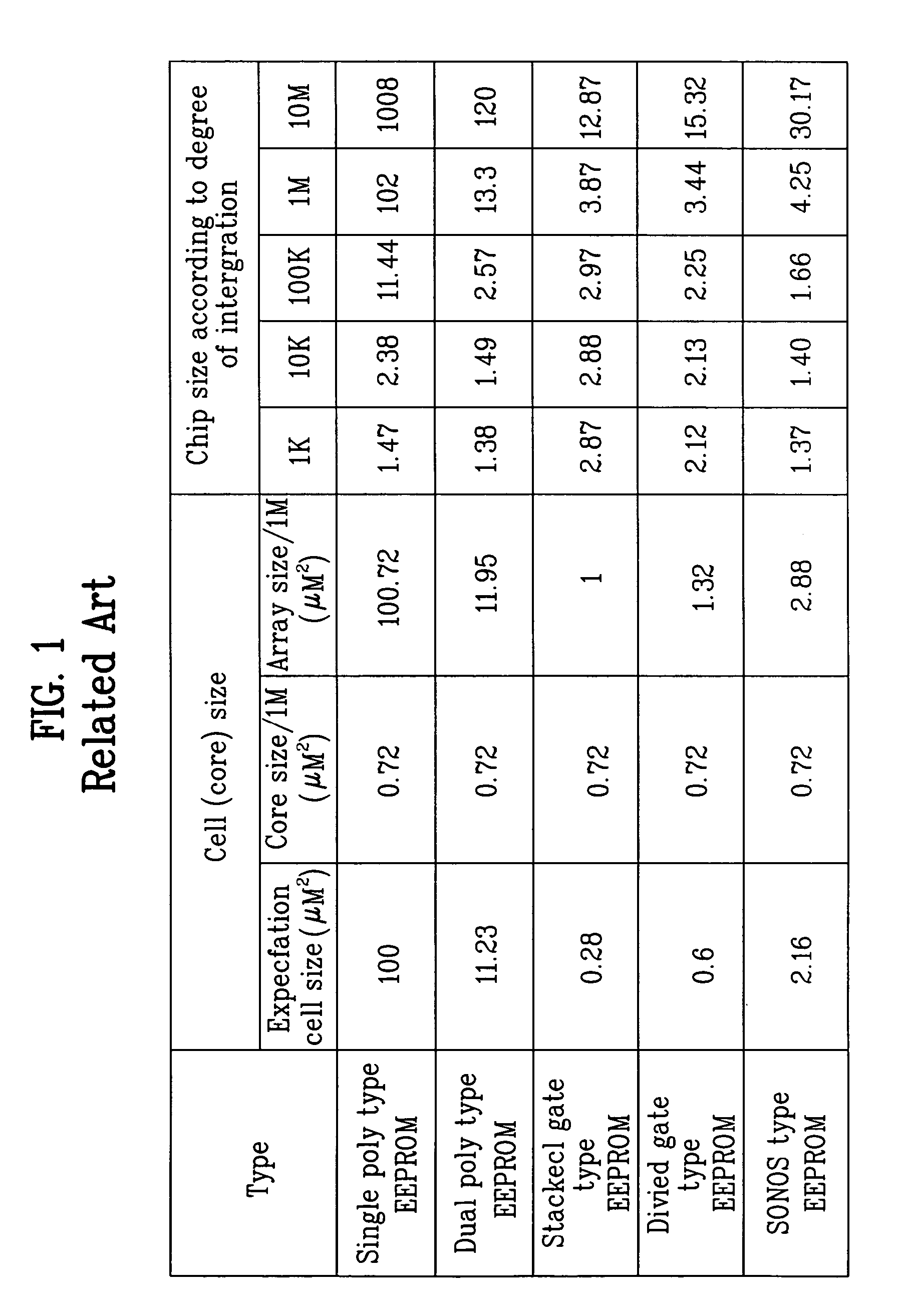
On the contrary, in case of the stacked gate type flash memory device, if the degree of cell integration becomes at least 1M, the corresponding fabrication is very complicated despite its high degree of integration.
However, even if the cell size, as shown in the table of FIG. 1, is relatively small in case of low integration degree, e.g., integration degree smaller than 10M, the cell size increases in case of the cell integration degree above 10M to weaken the competitiveness.

Method used


Image

  • Non-volatile memory device and fabricating method thereof
  • Non-volatile memory device and fabricating method thereof
  • Non-volatile memory device and fabricating method thereof

Examples


Embodiment Construction

[0040]Reference will now be made in detail to the preferred embodiments of the present invention, examples of which are illustrated in the accompanying drawings. Wherever possible, the same reference numbers will be used throughout the drawings to refer to the same or like parts.

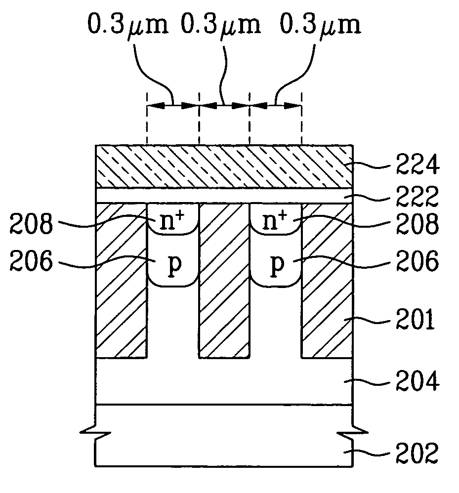
[0041]FIG. 6 is a layout of an embedded non-volatile memory device having the SONOS configuration according to the present invention. FIG. 7 and FIG. 8 are cross-sectional diagrams of the memory device bisected along cutting lines VII–VII′ and VIII–VIII′ in FIG. 6, respectively.

[0042]Referring to FIGS. 6 to 8, an n-well 204 is provided to an upper part of a semiconductor substrate 202 and an active area is defined in an upper part of the n-well 204 of the semiconductor substrate 202 by a trench isolating (TI) layer 201. And, a p-well 206 is arranged in the active area. A depth of the trench isolation layer 201 is minimum 5,000 Å and is preferably set to about 8,000 Å. A depth of the p-well 206 is smaller tha...


PUM


Abstract

The present invention provides a non-volatile memory device and fabricating method thereof, by which a cell size can be lowered despite high degree of cell integration and by which the device fabrication is facilitated. The present invention includes at least two trench isolation layers arranged in a device isolation area of a semiconductor substrate, each having a first depth, a first conductive type well arranged between the at least two trench isolation layers to have a second depth smaller than the first depth, a second conductive type source region and a second conductive type drain region arranged in a prescribed upper part of the first conductive type well to be separated from each other by a channel region in-between, an ONO layer on the channel region of the semiconductor substrate, the ONO layer comprising a lower oxide layer, a nitride layer, and an upper oxide layer, and a wordline conductor layer on the ONO layer.

Description

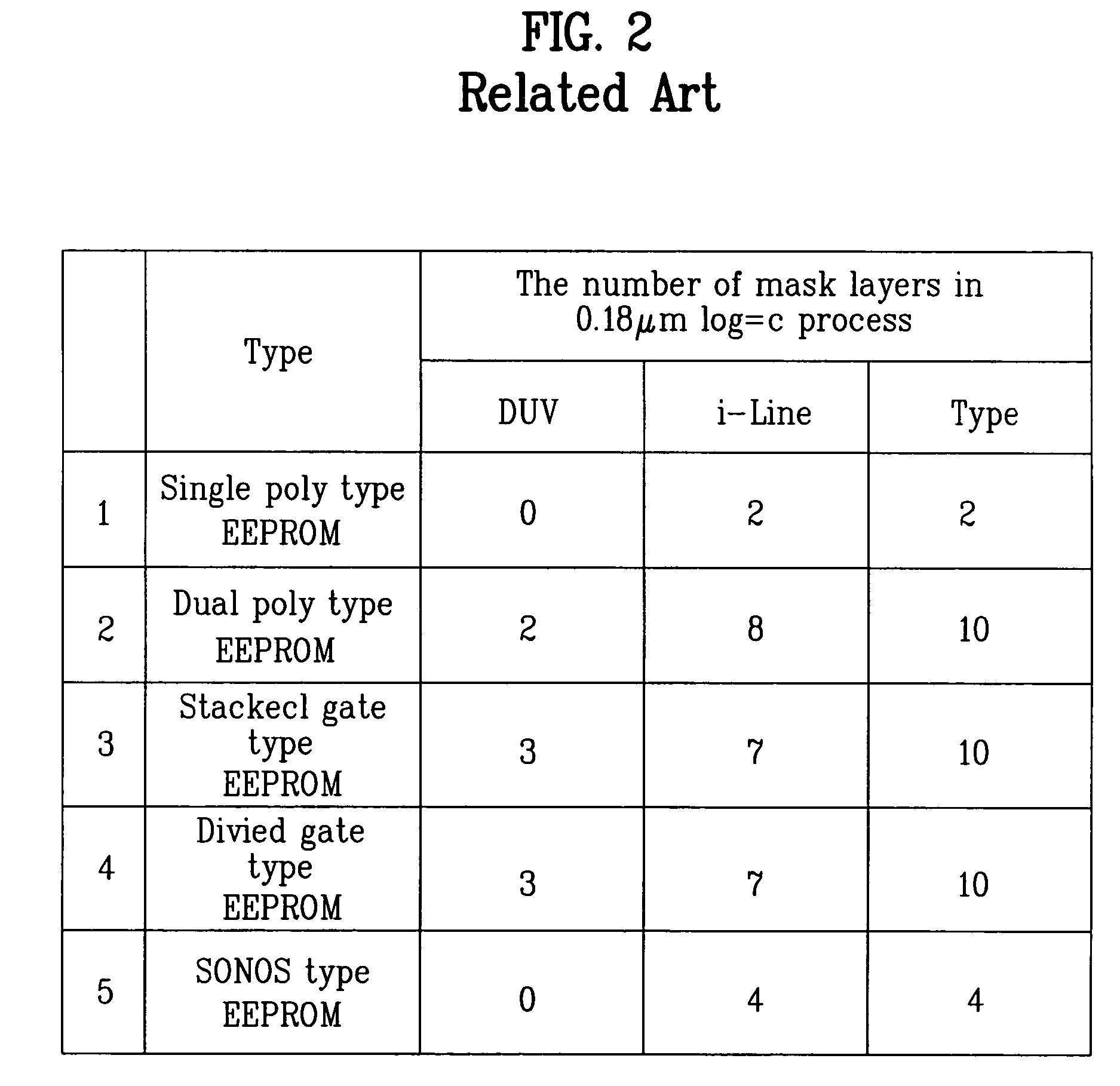
[0001]This application claims the benefit of the Korean Application No. P2003-0098361 filed on Dec. 27, 2003, which is hereby incorporated by reference.BACKGROUND OF THE INVENTION[0002]1. Field of the Invention[0003]The present invention relates to a non-volatile memory device and fabricating method thereof, and more particularly, to an embedded non-volatile memory device having a high integration degree and fabricating method thereof.[0004]2. Discussion of the Related Art[0005]Lately, developments for non-volatile memory devices capable of keeping data despite power cut-off are rapidly in progress. As non-volatile memory devices, there are single poly type EEPROM, dual poly type EEPROM, stacked gate type flash memory device, split gate type flash memory device, SONOS flash memory device, and the like. In many applications of the non-volatile memory devices, the embedded non-volatile memory device combining logic and memory therein employs various kinds of non-volatile memory device...

Claims


Application Information

Patent Timeline
Patent Type & Authority Patents(United States)
IPC IPC(8): H01L21/8238H01L21/336H01L29/792H10B12/00H10B20/00H10B69/00
CPCH01L27/115H01L29/792H01L29/66833H01L27/11568H10B43/30H10B69/00
Inventor JUNG, SUNG MUNKIM, JUM SOO
Owner DONGBU ELECTRONICS CO LTD
Learn More