High reverse voltage silicon carbide diode and method of manufacturing the same high reverse voltage silicon carbide diode

a silicon carbide diode, high reverse voltage technology, applied in the direction of semiconductor devices, semiconductor/solid-state device details, electrical apparatus, etc., can solve the problems of defect generation and increase of leakage current, and achieve the effect of increasing leakage curren

Inactive Publication Date: 2007-02-27
NISSAN MOTOR CO LTD
View PDF11 Cites 34 Cited by
  • Summary
  • Abstract
  • Description
  • Claims
  • Application Information

AI Technical Summary

Benefits of technology

[0005]However, defects are generated in the silicon carbide when the high energy ion implantation is performed, and this can easily become a cause for increase of the leakage current.

Problems solved by technology

However, defects are generated in the silicon carbide when the high energy ion implantation is performed, and this can easily become a cause for increase of the leakage current.

Method used


Image

  • High reverse voltage silicon carbide diode and method of manufacturing the same high reverse voltage silicon carbide diode
  • High reverse voltage silicon carbide diode and method of manufacturing the same high reverse voltage silicon carbide diode
  • High reverse voltage silicon carbide diode and method of manufacturing the same high reverse voltage silicon carbide diode

Examples


fourth embodiment

The Fourth Embodiment

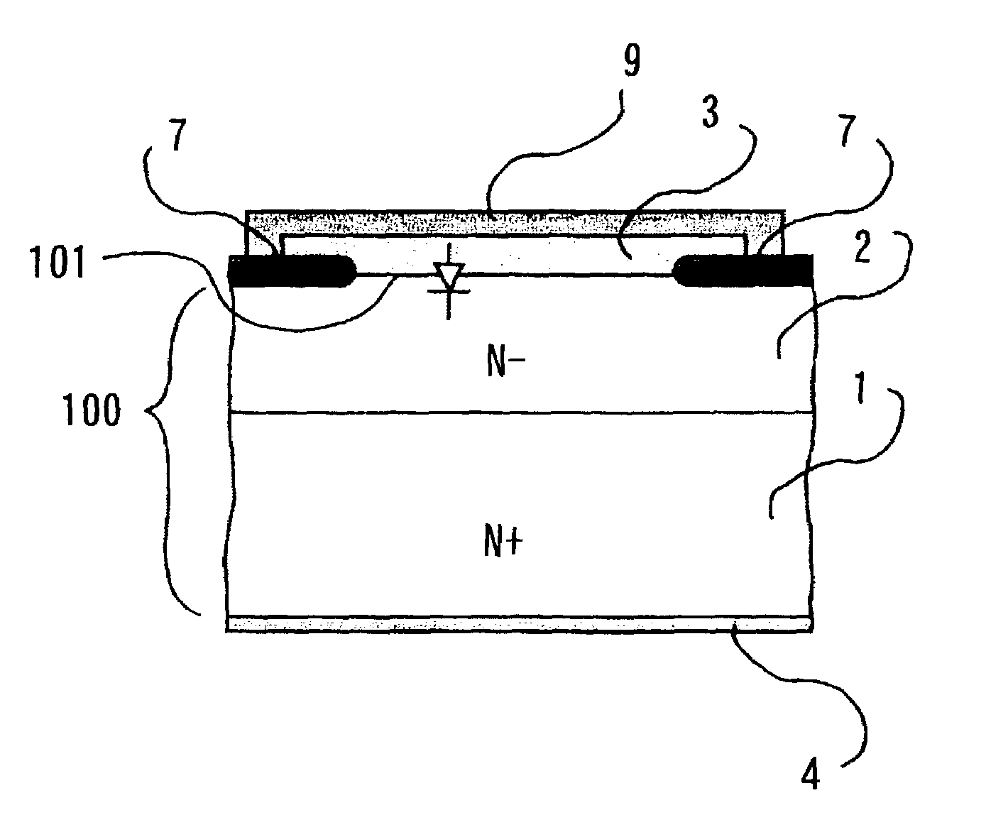
[0103]FIG. 16 shows the structure of the fourth preferred embodiment of the high reverse voltage silicon carbide diode according to the present invention. FIG. 16 is a cross sectional view corresponding to the portion shown in FIG. 6, by way of example, in which an epitaxial layer 2 made of low concentration N type silicon carbide and a polyclystalline silicon layer 3 are contacted together, and moreover a first surface electrode 9 is formed over the polycrystalline silicon layer 3. The point in which this structure differs from that of FIG. 6, is that a plurality of electric field relaxation regions 22 which are made of, for example, P type silicon carbide are formed within the silicon carbide base layer 100, in the vicinity of the hetero junction 101 which is formed by the polycrystalline silicon layer 3. These electric field relaxation regions 22 which are made of P type silicon carbide are arranged at predetermined intervals in the vicinity of the polycrysta...


PUM

PropertyMeasurementUnit
temperatureaaaaaaaaaa
thicknessaaaaaaaaaa
thicknessaaaaaaaaaa

Abstract

A high reverse voltage diode includes a hetero junction made up from a silicon carbide base layer, which constitutes a first semiconductor base layer, and a polycrystalline silicon layer, which constitutes a second semiconductor layer, and whose band gap is different from that of the silicon carbide base layer. A low concentration N type polycrystalline silicon layer is deposited on a first main surface side of the silicon carbide base layer, and a metal electrode is formed on a second main surface side of the silicon carbide base layer which is opposite to the first main surface side thereof.

Description

BACKGROUND OF THE INVENTION[0001]1. Field of the Invention[0002]The present invention relates to a high reverse voltage silicon carbide diode, and to a method of manufacturing the same high reverse voltage silicon carbide diode.[0003]2. Description of the Related Art[0004]A PN junction and a Schottky junction are per se known as prior art junctions for providing a high reverse voltage diode consisted of silicon carbide. It is necessary to form a deep diffusion region in order to obtain a high voltage capability by providing a PN junction to silicon carbide. Due to this, it is necessary to introduce the impurity by high energy ion implantation.SUMMARY OF THE INVENTION[0005]However, defects are generated in the silicon carbide when the high energy ion implantation is performed, and this can easily become a cause for increase of the leakage current.[0006]It would be desirable to provide a high reverse voltage silicon carbide diode and a method of manufacturing the same high reverse vol...

Claims


Application Information

Patent Timeline
Patent Type & Authority Patents(United States)
IPC IPC(8): H01L29/15H01L29/24H01L29/861
CPCH01L29/861H01L29/267H01L29/1608
Inventor SHIMOIDA, YOSHIOKANEKO, SAICHIROUTANAKA, HIDEAKIHOSHI, MASAKATSUTHRONGNUMCHAI, KRAISOMMIHARA, TERUYOSHIHAYASHI, TETSUYA
Owner NISSAN MOTOR CO LTD
Why Eureka
Try Eureka