Array substrate and manufacturing method thereof and display device

An array substrate and substrate technology, applied in optics, instruments, electrical components, etc., can solve the problems of liquid crystal displays such as greenish horizontal gray scale, lower transmittance, uneven display, etc., to improve picture quality, prevent light exposure, Improve the effect of horizontal grayscale unevenness

Active Publication Date: 2013-09-18
BOE TECH GRP CO LTD
View PDF6 Cites 30 Cited by
  • Summary
  • Abstract
  • Description
  • Claims
  • Application Information

AI Technical Summary

Problems solved by technology

[0006] The technical problem to be solved by the present invention is to provide an array substrate, its manufacturing method, and a display device, which can solve the problems of greenish and uneven horizontal gray levels (X- Talk) and other poor display problems, improve the picture quality of display devices, especially high-resolution products

Method used


Image

  • Array substrate and manufacturing method thereof and display device
  • Array substrate and manufacturing method thereof and display device
  • Array substrate and manufacturing method thereof and display device

Examples


Embodiment 1

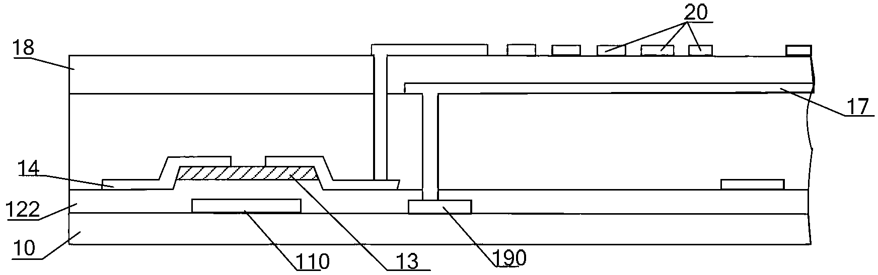
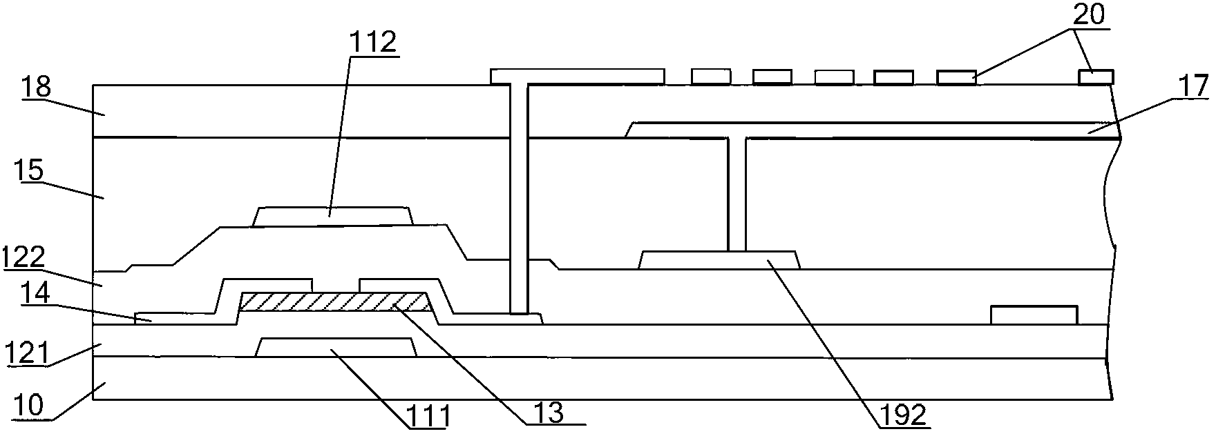
[0055] An embodiment of the present invention provides an array substrate, such as figure 2 As shown, the array substrate includes: a substrate 10, a semiconductor layer 13, a source-drain electrode layer 14, and a gate insulating layer 122 sequentially arranged on the substrate from bottom to top, and also includes:

[0056] a first gate metal layer 112 disposed on the gate insulating layer 122;

[0057] the second gate insulating layer 121 disposed under the semiconductor layer 13; and,

[0058]The second gate metal layer 111 is disposed between the second gate insulating layer 121 and the substrate 10 .

[0059] Wherein, the second gate metal layer 111 and the first gate metal layer 112 may also be made of the same material, such as one or more selected from molybdenum, aluminum, chromium, and copper. The second gate insulating layer 121 and the gate insulating layer 122 may also be made of the same material, for example, both may be silicon nitride films, and of course ...

Embodiment 2

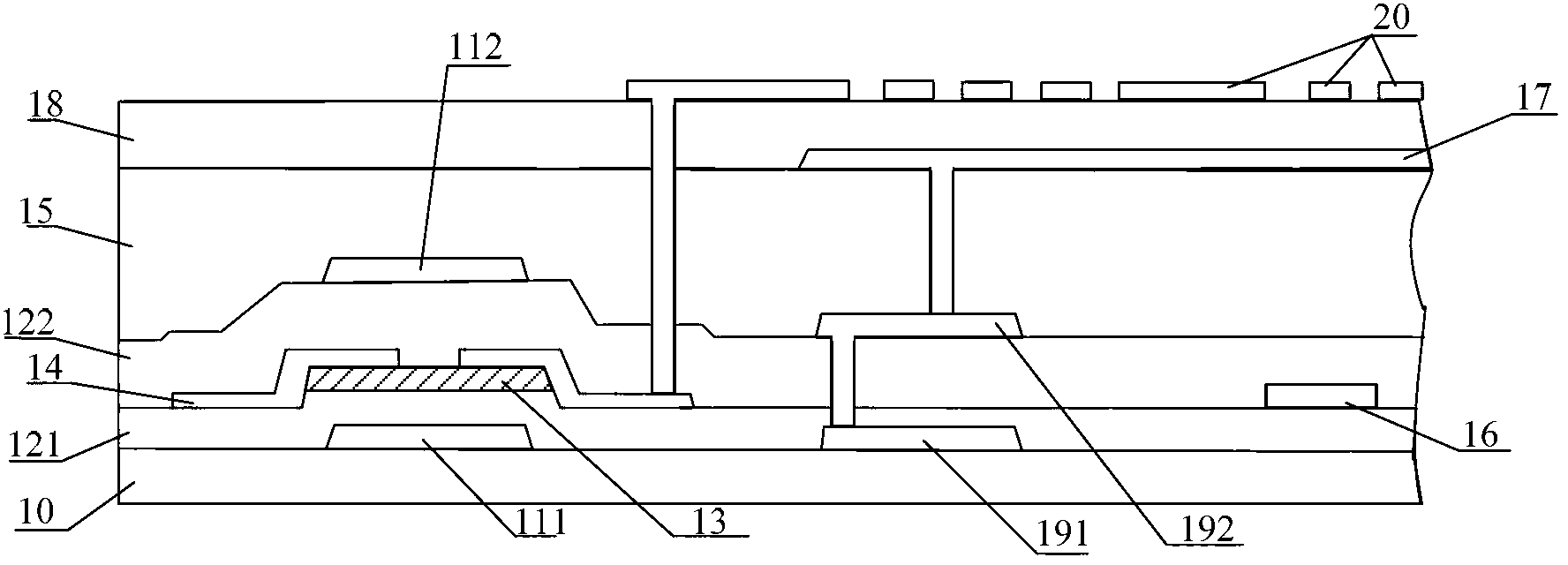
[0070] An embodiment of the present invention provides an array substrate, and figure 2 The difference of Embodiment 1 is that the array substrate further includes: a second common electrode line,

[0071] When the first common electrode line is on the same layer as the first gate metal layer, the second common electrode line is on the same layer as the second gate metal layer; when the first common electrode line is on the same layer as the first gate metal layer; When the second gate metal layer is on the same layer, the second common electrode line is on the same layer as the first gate metal layer;

[0072] The second common electrode line is connected to the first common electrode line through the insulating layer and via holes in the gate insulating layer.

[0073] In order to better understand this embodiment, a specific implementation manner of this embodiment is given here, such as image 3 As shown, the array substrate includes: a substrate 10, a second gate metal...

Embodiment 3

[0088] An embodiment of the present invention also provides a display device, which includes any one of the array substrates described in Embodiments 1 and 2. The display device may be any product or component with a display function such as a liquid crystal panel, an electronic paper, an OLED panel, a mobile phone, a tablet computer, a television set, a monitor, a notebook computer, a digital photo frame, a navigator, and the like.

[0089] The display device described in this embodiment uses the array substrate of the present invention, so it can improve the display defects such as greenish and horizontal X-talk in the display device without reducing the transmittance. , the display effect is improved.


PUM


Abstract

The invention discloses an array substrate and a manufacturing method thereof and a display device, relates to the field of display, and can solve the bad display problems of greenish phenomenon, horizontal X-talk and the like of a liquid crystal display and improve the image quality of the display device, in particular a high-resolution product on the premise of not reducing the transmittance rate. The array substrate comprises a substrate, a semiconductor layer, source and drain electrode layers, a grid insulation layer, a first grid metal layer, a second grid insulation layer and a second grid metal layer, wherein the semiconductor layer, the source and drain electrode layers and the grid insulation layer are arranged on the substrate in sequence from bottom up; the first grid metal layer is arranged on the grid insulation layer; the second grid insulation layer is arranged below the semiconductor layer; and the second grid metal layer is arranged between the second grid insulation layer and the substrate.

Description

technical field [0001] The present invention relates to the display field, in particular to an array substrate, a manufacturing method thereof, and a display device. Background technique [0002] Due to its advantages of light weight, low power consumption, low radiation, and a large amount of space saving, liquid crystal displays have replaced traditional cathode ray tube displays and are widely used in various display fields, such as households, public places, offices, and personal electronics. products etc. [0003] like figure 1 As shown, the existing liquid crystal display includes display pixels (units) and thin film transistors (TFTs) for controlling loading of display data. Among them, the thin-film transistor generally adopts a bottom-gate structure (the gate of the thin-film transistor is located below the semiconductor layer 13), specifically including: a substrate 10, a gate metal layer 110 arranged on the substrate 10 from top to bottom, and a gate insulating ...

Claims


Application Information

Patent Timeline
Patent Type & Authority Applications(China)
IPC IPC(8): G02F1/1368
CPCG02F1/134363G02F1/136227G02F1/134372H01L27/1255H01L29/78633H01L29/78648G02F1/1368H01L27/124H01L27/1248H01L27/1288H01L29/41733
Inventor 崔贤植李会徐智强严允晟
Owner BOE TECH GRP CO LTD
Why Eureka
Try Eureka