

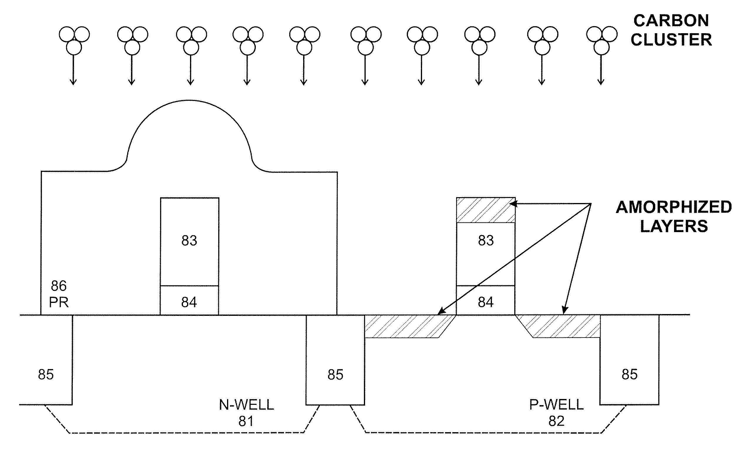
System and method for the manufacture of semiconductor devices by the implantation of carbon clusters
Carbon cluster implantation in semiconductor manufacturing addresses the challenge of boron diffusion and channeling in PMOS transistors by amorphizing the silicon lattice, enhancing transistor performance and wafer throughput, and allowing for standard annealing processes, thus improving junction formation and reducing thermal budgets.
- Summary
- Abstract
- Description
- Claims
- Application Information
AI Technical Summary
Benefits of technology
Problems solved by technology
Method used
Image

Examples
Embodiment Construction
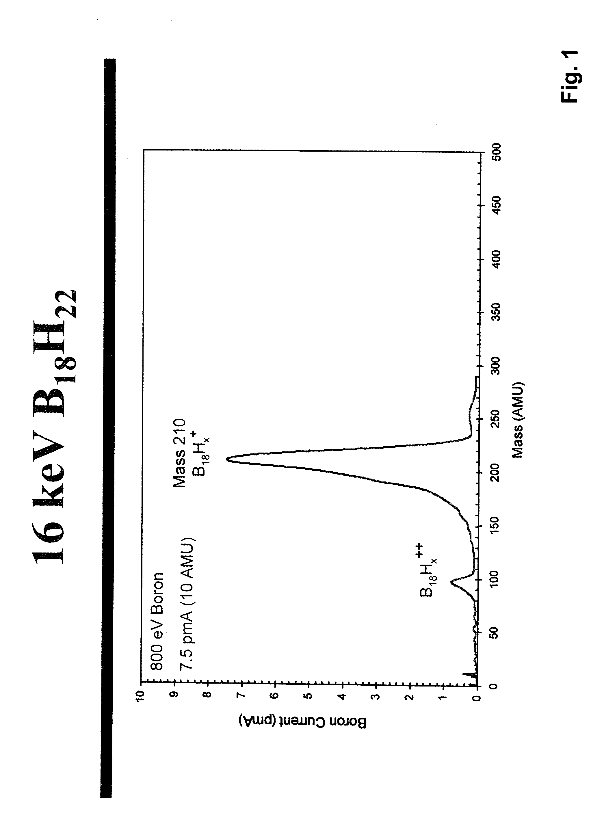
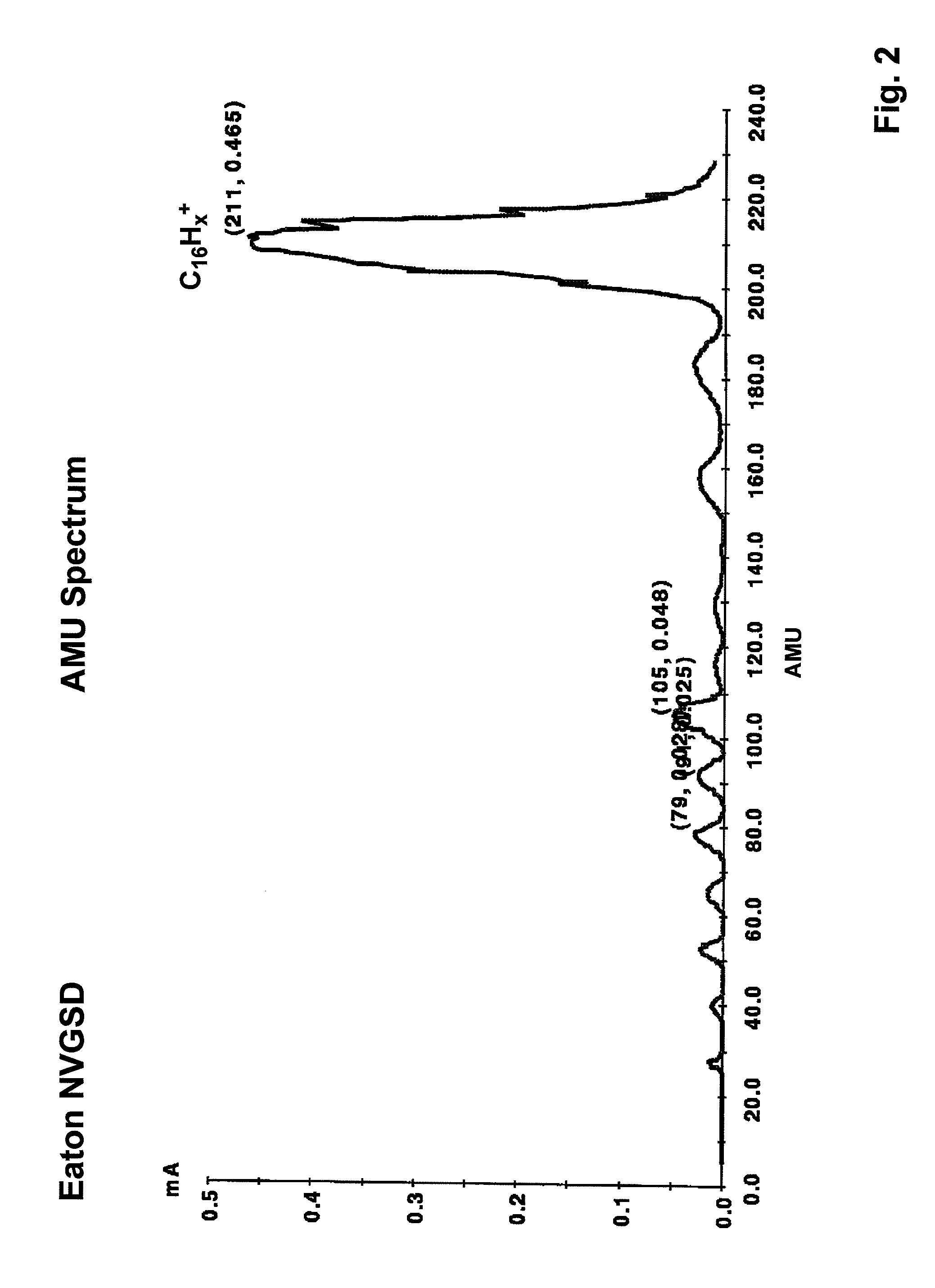
[0071]FIG. 1 shows a mass spectrum of B18H22 as produced by an ion implantation system. A Clusterlon® source, for example, as mentioned above, is used to generate ions which are extracted at 20 kV and transported through an analyzer magnet. A resolving aperture at the exist of the magnet provided a modest mass resolution of M / ΔM=15; the beam is scanned across the resolving aperture and the ion current is passed the resolving aperture and measured by a Faraday located about 2 meters from the source. The parent peak at 210 amu is composed of B18Hx+; there is a range of retained H atoms of perhaps 1016H10, as produced by an ion implantation system. The parent peak C16Hx+ is at 211 amu, and the Faraday current was about 500 uA at 17 kV extraction voltage. Thus, the effective implant energy per carbon atom was about 1 keV, and the effective carbon current about 8 mA. Note that the mass, effective current, and implantation energy of the C of FIG. 2 and B of FIG. 1 are about the same. The ...
PUM
 Abstract
Description
Claims
Application Information