Electrical-interference-isolated transistor structure

a transistor and isolation technology, applied in the direction of semiconductor devices, electrical equipment, semiconductor/solid-state device details, etc., can solve the problems of adverse influences on the stability of the whole electronic system, noise, and noise, etc., to improve the chip packaging structure, isolate electrical noise, and reduce electromagnetic interferen

Inactive Publication Date: 2007-03-06
DOMINTECH
View PDF3 Cites 69 Cited by
  • Summary
  • Abstract
  • Description
  • Claims
  • Application Information

AI Technical Summary

Benefits of technology

[0005]A primary object of the present invention is to provide an electrical-interference-isolated transistor structure that has an improved chip packaging structure to isolate electrical noises, reduce electromagnetic interferences, improve transmission rate, strengthen chip packaging structure, serve as a common grounding circuit, and achieve an improved rate of heat release.
[0006]To achieve the above and other objects, the transistor structure of the present invention includes at least one chip; a packaging insulating layer, a first adhesive layer, a conducting layer, and a second adhesive layer sequentially provided on one side of the chip having electrical contacts provided thereon, so that the conducting layer is bonded between the first and the second adhesive layer; and a leadframe bonded to an outer side of the second adhesive layer. The conducting layer may be a metal sheet, a metal film, or a type of conducting fiber. The leadframe is electrically connected to the electrical contacts on the chip via lead wires, and at least one of the electrical contacts on the chip is electrically connected to the conducting layer via a conductor, so that the conducting layer is able to isolate electrical noises, reduce the electromagnetic interferences, improve the transmission rate, strengthen the chip packaging structure, serve as a common grounding circuit, and improve the rate of heat release in the whole transistor structure.

Problems solved by technology

It is known that electronic products in operation produce electromagnetic interferences (EMI), noises, including shot noise, flicker noise, surge noise, thermal noise, partition noise, etc., and high temperature.
Most of the noises are produced due to electromagnetic interference and have adverse influences on the stability of the whole electronic system.
However, the above-described conventional chip packaging structure does not include any structural design for preventing electromagnetic interference to meet the high standard of electromagnetic compatibility required by current electronic products.

Method used


Image

  • Electrical-interference-isolated transistor structure
  • Electrical-interference-isolated transistor structure
  • Electrical-interference-isolated transistor structure

Examples


Embodiment Construction

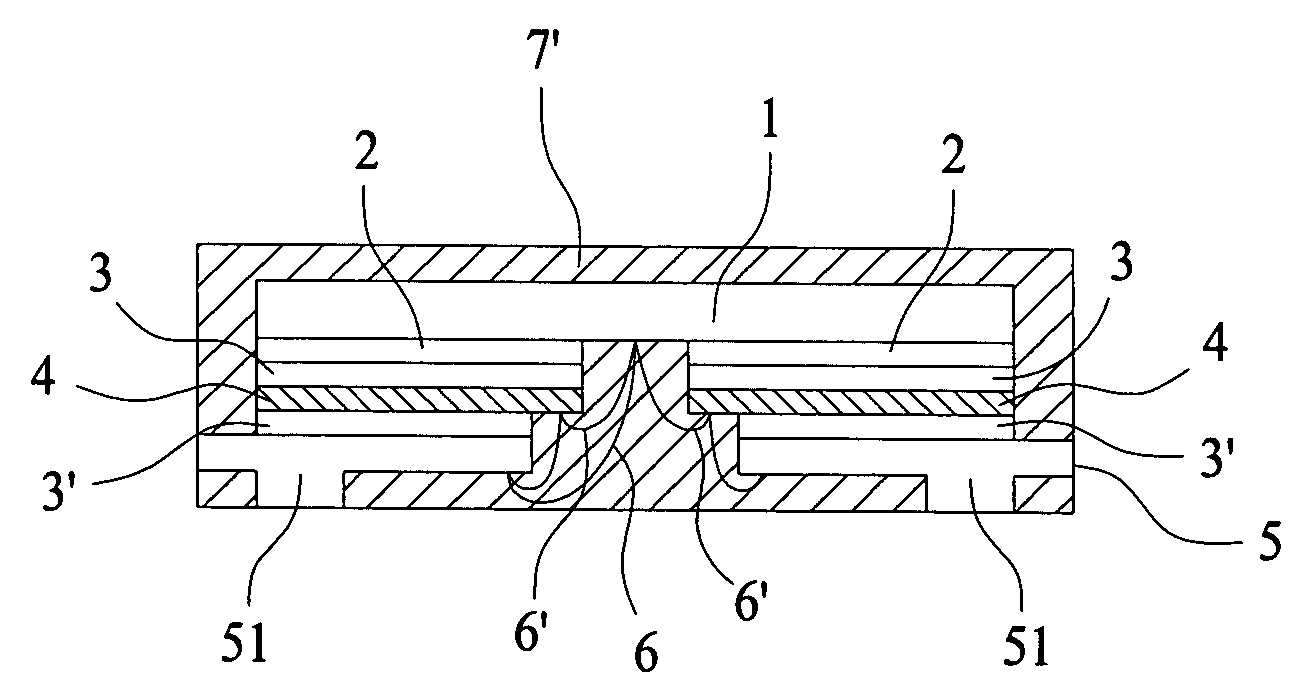
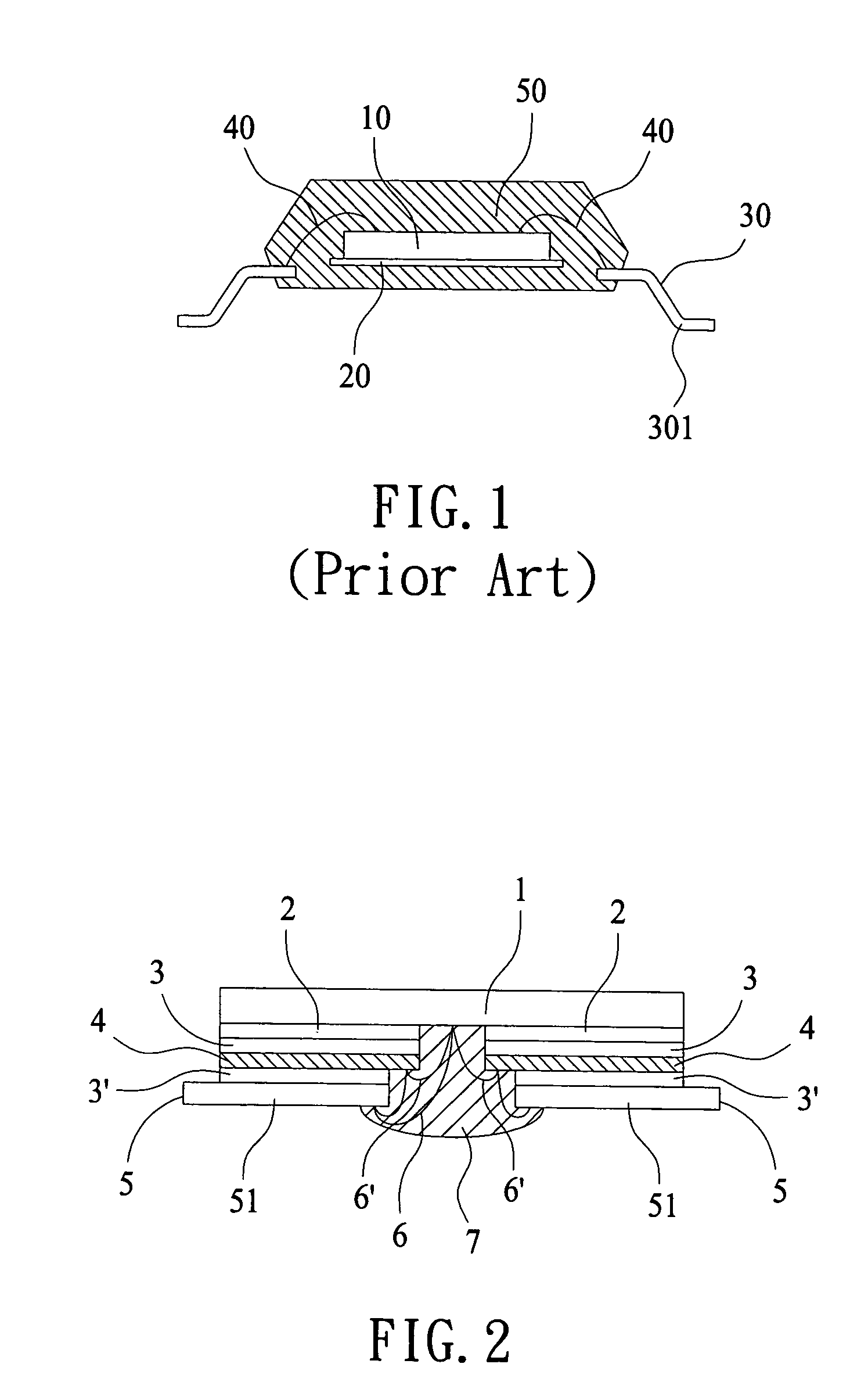
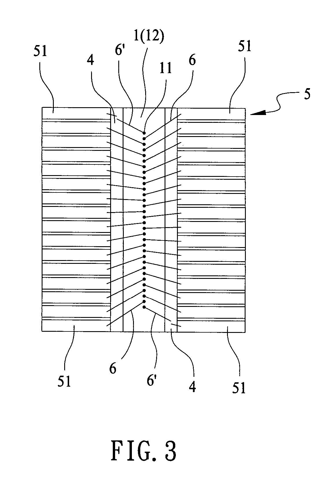
[0015]Please refer to FIGS. 2, 3, and 4 in which an electrical-interference-isolated transistor structure according to a preferred embodiment of the present invention is shown. As shown, the transistor structure of the present invention in this preferred embodiment mainly includes a chip 1, an optional packaging insulating layer 2, a first and a second adhesive layer 3, 3′, a conducting layer 4, a leadframe 5, lead wires 6 and conductors 6′ connecting the chip 1 to the conducting layer 4 and the leadframe 5, and a sealing material 7.

[0016]The chip 1, which is a known product and is therefore not discussed in any details herein, has one side provided with electrical contacts 11. The optional packaging insulating layer 2, the first adhesive layer 3, the conducting layer 4, and the second adhesive layer 3′ are sequentially arranged on the chip 1 at the side with the electrical contacts 11 from inner to outer side, so that the conducting layer 4 is fixedly bonded between the first and t...


PUM


Abstract

A transistor structure includes at least one chip; a packaging insulating layer, a first adhesive layer, a conducting layer, and a second adhesive layer sequentially provided on one side of the chip having electrical contacts thereon, so that the conducting layer is bonded between the first and the second adhesive layer; and a leadframe bonded to an outer side of the second adhesive layer. The conducting layer may be a metal sheet, a metal film, or a type of conducting fiber. The leadframe is connected to the electrical contacts on the chip via lead wires, and at least one of the electrical contacts on the chip is connected to the conducting layer via a conductor, so that the conducting layer is able to isolate electrical noises and reduce electromagnetic interferences, improve rates of transmission and heat release, strengthen chip packaging structure, and serve as a common grounding circuit.

Description

FIELD OF THE INVENTION[0001]The present invention relates to an electrical-interference-isolated transistor structure, and more particularly to a chip packaging structure that includes shielding and grounding structure to enable reduced electrical noise interference and improved rate of heat release thereof.BACKGROUND OF THE INVENTION[0002]FIG. 1 is a sectional view of a conventional chip packaging structure, in which a chip 10 is positioned on a chip pad 20 and a leadframe 30 is provided at each lateral side of the chip 10 to electrically connect with external elements. Each leadframe 30 includes a plurality of sequentially arranged terminal legs 301, which are connected to contacts on the chip 10 via gold wires 40. An insulating sealing material 50 is applied to enclose the chip 10 and thereby protects and locates the chip 10, the gold wires 40, and other internal elements in place.[0003]It is known that electronic products in operation produce electromagnetic interferences (EMI),...

Claims


Application Information

Patent Timeline
Patent Type & Authority Patents(United States)
IPC IPC(8): H01L23/495
CPCH01L23/49524H01L24/06H01L24/49H01L23/4951H01L23/3107H01L24/48H01L24/45H01L2224/04042H01L2224/05553H01L2224/05599H01L2224/06136H01L2224/45144H01L2224/48091H01L2224/4824H01L2224/48247H01L2224/49109H01L2224/49171H01L2224/85399H01L2924/01079H01L2924/01082H01L2924/3025H01L2924/01033H01L2924/00014H01L2224/48599H01L2224/73215H01L2924/00H01L2924/181H01L2924/10162H01L2924/00012
Inventor TZU, CHUNG-HSINGCHANG, SHIH-YI
Owner DOMINTECH
Why Eureka
Try Eureka