Circular chemiresistors for microchemical sensors

a microchemical sensor and chemiresistors technology, applied in the direction of instruments, specific gravity measurement, calibration apparatus, etc., can solve the problems of clogging, difficult precise placement and volume control, and uncontrollable parameters, so as to minimize batch-to-batch variations in baseline resistance, the effect of maximizing the contact area

Inactive Publication Date: 2007-03-13
SANDIA NAT LAB
View PDF8 Cites 106 Cited by
  • Summary
  • Abstract
  • Description
  • Claims
  • Application Information

AI Technical Summary

Benefits of technology

[0028]The present invention relates to a circular chemiresistor for use in microchemical sensors. A pair of electrodes is fabricated on an electrically insulating substrate. The pattern of electrodes is arranged in a circle-filling geometry, such as a concentric, dual-track spiral design, or a circular interdigitated design. A drop of a chemically sensitive polymer (i.e., chemiresistive ink) is deposited on the insulating substrate on top of the pair of electrodes, which spreads out into a thin, circular disk contacting the pair electrodes. This circularly-shaped electrode geometry maximizes the contact area between the pair of electrodes and the polymer deposit, which provides a lower and more stable baseline resistance than with linear-trace designs. The circularly shaped electrode pattern also serves to minimize batch-to-batch variations in the baseline resistance due to non-uniform distributions of conductive particles in the chemiresistive polymer film.

Problems solved by technology

Unfortunately, these parameters are not well controlled using current methods of solvent casting.
Precise placement and volume control is challenging.
In the fabrication of chemiresistor-type microchemical sensors (where conductive particles are dispersed within a polymer matrix), clogging can occur if the solvent dries while the chemiresistive ink is introduced or stored in the machine, or while the ink is being ejected from the machine.
This creates unacceptable variability in the conductive particle / polymer ratio, which directly affects the repeatability and performance of chemiresistors; as well as reducing the production yields (e.g., yields greater than 30% are difficult to achieve due to nozzle clogging with automatic machines).
Filters can be used to help reduce clogging, but then the filters get clogged.
Manual techniques, such as hand painting, brushing, dabbing, etc. have been used, but suffer from poor reproducibility and imprecise placement.
Hence, it is not uncommon for the baseline electrical resistance of these manually placed polymer composite films to vary by factors of 2–3, which is clearly unacceptable for commercial manufacture.
However, despite the use of a micropipette tool to deposit nominally “circular” films having a diameter of approximately 1.5–2.5 mm, the edges and composition of the deposited films are also irregular and non-uniform.
Additionally, a large amount of excess material has been deposited on either side of the four parallel electrodes, which causes an unnecessary waste of material.
Also, the overall pattern of electrode traces on the substrate (i.e., silicon die) is not particularly compact; since about 50% of the electrode's length is not covered by the chemically sensitive film.
The lower the contact area ratio is, the greater the sensitivity of the chemiresistor will be to errors caused by any detachment of the polymer matrix from the electrodes.
Lewis and Freund, however, do not discuss the practical problems of obtaining reproducible and reliable performance, with high manufacturing yields, when depositing realistic polymer composite films having less-than-ideal shapes, thickness variations, and non-uniform composition, etc.

Method used


Image

  • Circular chemiresistors for microchemical sensors
  • Circular chemiresistors for microchemical sensors
  • Circular chemiresistors for microchemical sensors

Examples


Embodiment Construction

[0082]The words “vapor” and “gas” are used interchangeably herein. Similarly, the acronym VOC, which stands for Volatile Organic Compound, is intended herein to also encompass all inorganic volatile compounds (VCs), other solvents, volatile toxic chemicals, volatile explosives, and organic compounds even having low volatility.

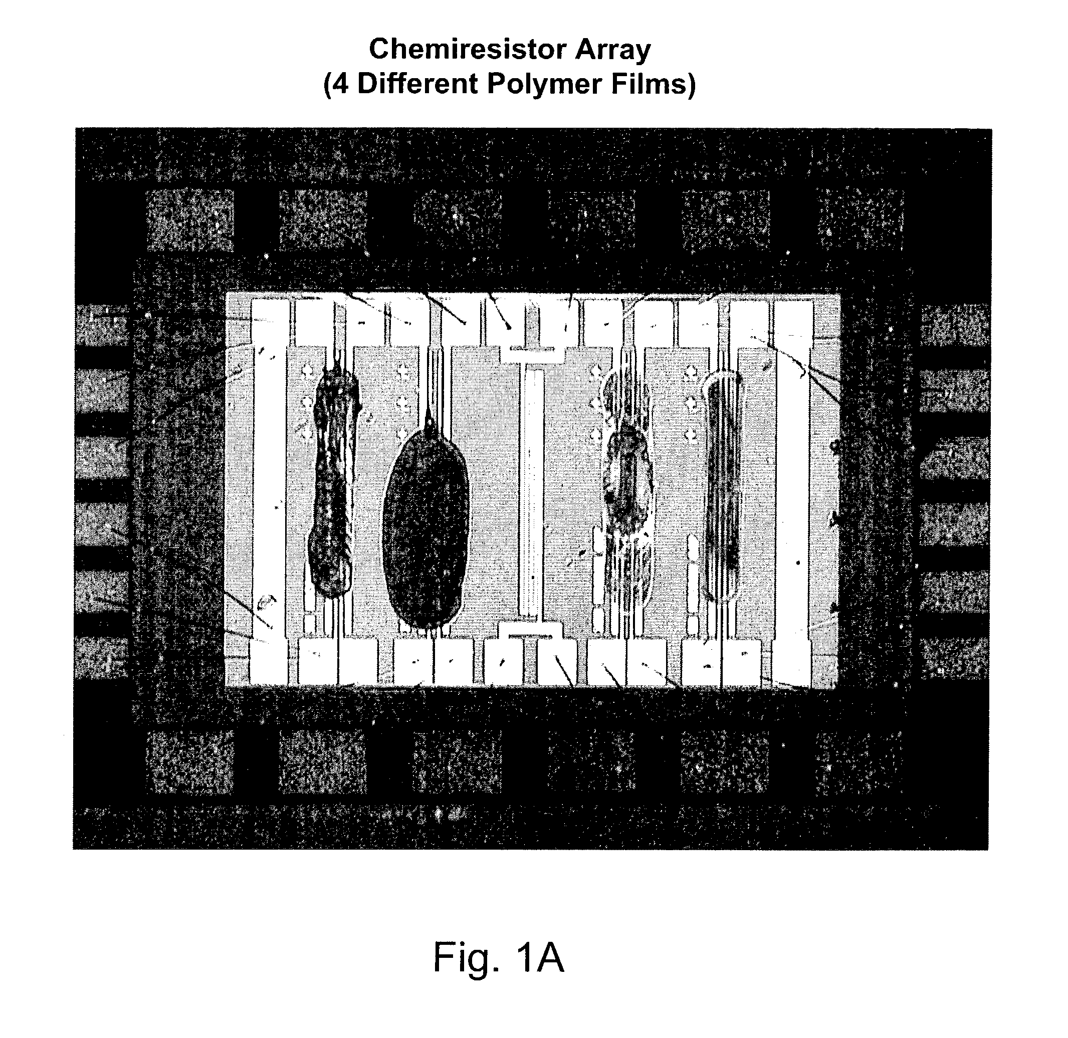
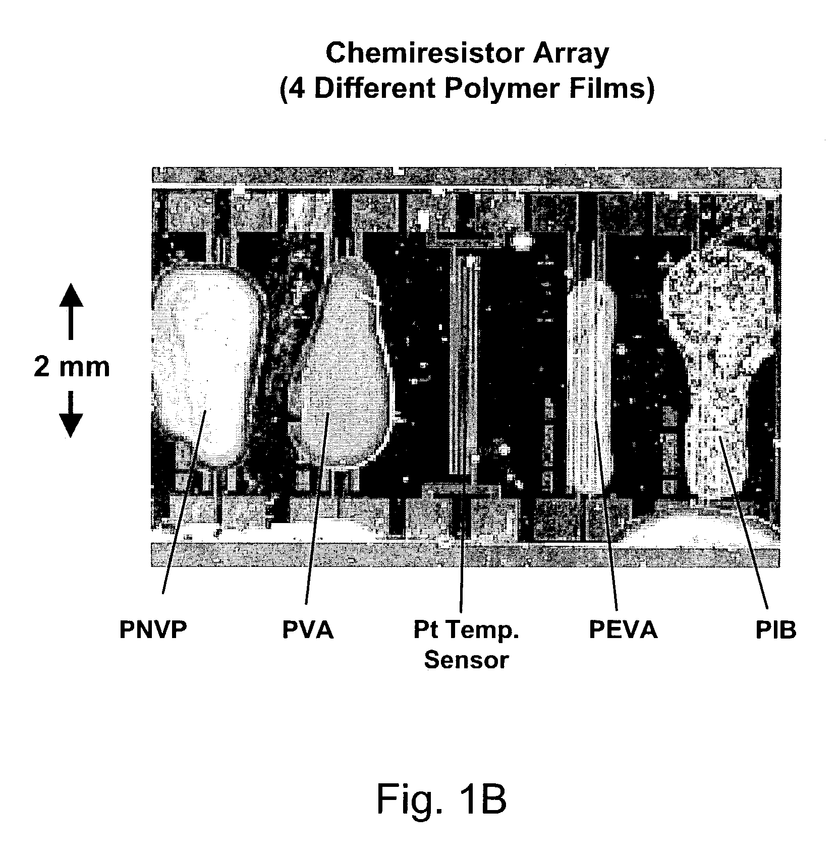
[0083]The words “polymer film”, “polymer coating”, “chemically sensitive polymer film”, “polymer composite”, “chemically sensitive polymer deposit”, “polymer deposit”, unless otherwise defined, all refer to the disc of chemiresistive ink after it has been deposited on a substrate and dried.

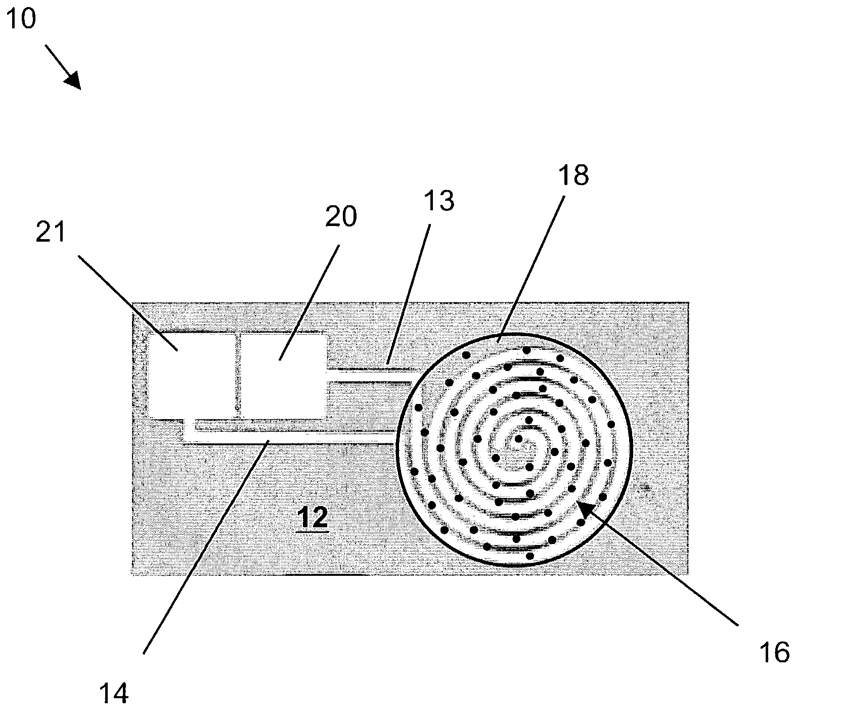
[0084]FIG. 4a illustrates a schematic plan view of a first example of a circular chemiresistor, according to the present invention. Circular chemiresistor 10 comprises an electrically insulating substrate 12 with a pair of conductive lines 13, 14 disposed on the substrate, with each line having a distal end. The pair of distal ends conductive lines 13, 14 are arranged in a ci...


PUM

PropertyMeasurementUnit
diameteraaaaaaaaaa
widthaaaaaaaaaa
diameteraaaaaaaaaa

Abstract

A circular chemiresistor for use in microchemical sensors. A pair of electrodes is fabricated on an electrically insulating substrate. The pattern of electrodes is arranged in a circle-filling geometry, such as a concentric, dual-track spiral design, or a circular interdigitated design. A drop of a chemically sensitive polymer (i.e., chemiresistive ink) is deposited on the insulating substrate on the electrodes, which spreads out into a thin, circular disk contacting the pair of electrodes. This circularly-shaped electrode geometry maximizes the contact area between the pair of electrodes and the polymer deposit, which provides a lower and more stable baseline resistance than with linear-trace designs. The circularly-shaped electrode pattern also serves to minimize batch-to-batch variations in the baseline resistance due to non-uniform distributions of conductive particles in the chemiresistive polymer film.

Description

CROSS-REFERENCE TO RELATED APPLICATIONS[0001]This application claims the benefit of U.S. Provisional patent application Ser. No. 60 / 351,535 “Novel Designs and Deposition Methods for Polymer-Based Microchemical Sensors”, by Clifford K. Ho, filed Jan. 24, 2002, which is incorporated herein by reference. This application is related to co-pending application Ser. No. 09 / 974,327, “Apparatus for Sensing Volatile Organic Chemicals in Fluids”, by Hughes, et al, which is incorporated herein by reference. This application is related to co-pending application, “Confined Cavity Chemiresistors for Microchemical Sensors”, by Clifford K. Ho, filed Jan. 23, 2003. This application is related to co-pending application, “Multi-Pin Chemiresistors for Microchemical Sensors”, by Clifford K. Ho, filed Jan. 23, 2003.FEDERALLY SPONSORED RESEARCH[0002]The United States Government has rights in this invention pursuant to Department of Energy Contract No. DE-AC04-94AL85000 with Sandia Corporation.BACKGROUND OF...

Claims


Application Information

Patent Timeline
Patent Type & Authority Patents(United States)
IPC IPC(8): B32B5/02B32B27/04B32B27/12G01N15/06G01N25/18
CPCG01N27/126Y10T29/49002
Inventor HO, CLIFFORD K.
Owner SANDIA NAT LAB
Why Eureka
Try Eureka