Cascade wake-up circuit preventing power noise in memory device

a wake-up circuit and memory device technology, applied in the field of memory devices, can solve the problems of data loss of memory cells, multiple sources of noise, and large amount of peak current generation

Active Publication Date: 2007-03-20
SAMSUNG ELECTRONICS CO LTD
View PDF8 Cites 113 Cited by
  • Summary
  • Abstract
  • Description
  • Claims
  • Application Information

AI Technical Summary

Problems solved by technology

There are several sources of noise when a semiconductor memory device operates.
A peak current, which is generated when discharged parts of a circuit are simultaneously precharged, is a typical source if such noise.
One of the primary considerations regarding the type of memory that is commonly used in portable telephone systems is amount of loss due to leakage current.
However, a large amount of peak current is generated during a wake-up operation in which the memory device transitions from a sleep mode to an active mode.
In a worst-case scenario, the power supply voltage can drop below a retention voltage of the memory cell, which can therefore result in data loss of the memory cell.
During this operation, a peak current is generated, in turn causing a voltage drop.
That is, data of the SRAM bit cell is threatened by the IR drop occurring due to the reduction of the power supply voltage.
Therefore, the peak currents may not be properly distributed.
Also, when the delay time of the inverter chains 26, 28, are increased to preserve data of the memory cell, timing loss can result from an increased wake-up timing margin.
Alternatively, when the delay time in the inverter chain is increased by increasing the number of inverters, the overall time required for the wake-up operation is increased.

Method used


Image

  • Cascade wake-up circuit preventing power noise in memory device
  • Cascade wake-up circuit preventing power noise in memory device
  • Cascade wake-up circuit preventing power noise in memory device

Examples


Embodiment Construction

[0046]The present invention will now be described more fully with reference to the accompanying drawings, in which embodiments of the invention are shown.

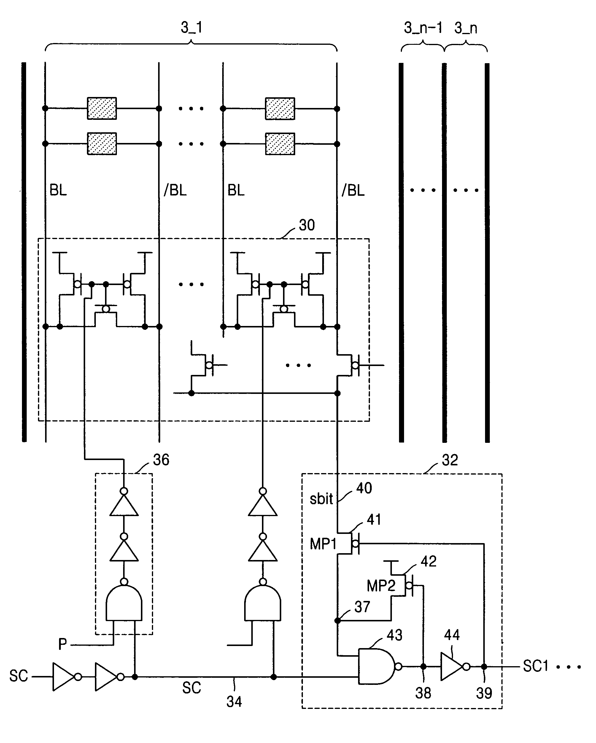
[0047]In the present invention, a cascade-type wake-up circuit is provided in which a subsequent block is placed in a wake-up mode after a previous block has been placed in wake-up mode. Further, the wake-up circuit of the present invention is smaller in size than a conventional wake-up circuit of the type including an inverter chain. In addition, the wake up circuit of the present invention can detect a change in a wake-up delay caused by certain processes, and can thereby control the peak current by using a bit line of a previous block as an input of a NAND feedback structure. Also, the wake-up circuit affects only the wake-up operation of the memory device and does not influence the performance of other system operations.

[0048]FIG. 5 is a circuit diagram of a wake-up circuit of an SRAM device according to an embodiment of the pr...


PUM


Abstract

A wake-up circuit of a memory device employs a cascade chain structure in which bit lines are divided into a plurality of blocks, and if the bit lines of one of the blocks are determined to have undergone a wake-up operation based on a bit line voltage fed back in the block, the wake-up operation is performed on a subsequent block. Accordingly, a wake-up delay can be varied, and therefore peak currents can be controlled, thereby reducing overall system power noise.

Description

BACKGROUND OF THE INVENTION[0001]This application claims the priority of Korean Patent Application No. 2004-48041, filed on Jun. 25, 2004, in the Korean Intellectual Property Office, the disclosure of which is incorporated herein in its entirety by reference.[0002]1. Field of the Invention[0003]The present invention relates to a memory device, and more particularly, to a wake-up method of and a wake-up circuit for converting a sleep mode to an active mode in a memory device.[0004]2. Description of the Related Art[0005]In a semiconductor memory device, it is very important to prevent malfunction that is generated as a result of noise in the power supply. There are several sources of noise when a semiconductor memory device operates. A peak current, which is generated when discharged parts of a circuit are simultaneously precharged, is a typical source if such noise.[0006]In particular, in a memory cell array, there is a high possibility that large peak currents will be generated in a...

Claims


Application Information

Patent Timeline
Patent Type & Authority Patents(United States)
IPC IPC(8): G11C5/14G11C7/00G11C7/12G11C7/20G11C7/22
CPCG11C7/20G11C7/22G11C2207/2227G11C7/12G11C5/14
Inventor CHOI, HYUN-SUKIM, KYEONG-RAE
Owner SAMSUNG ELECTRONICS CO LTD
Why Eureka
Try Eureka