Organic devices having a fiber structure

a fiber structure and optoelectronic technology, applied in the manufacture of cladded optical fibers, instruments, final products, etc., can solve the problems of difficult and expensive production of efficient crystalline-based devices, not providing signal or current to control detection circuitry, and not providing power to devices, equipment, devices or equipmen

Active Publication Date: 2007-03-20
THE TRUSTEES FOR PRINCETON UNIV
View PDF31 Cites 44 Cited by
  • Summary
  • Abstract
  • Description
  • Claims
  • Application Information

AI Technical Summary

Problems solved by technology

As a general rule, a photovoltaic cell provides power to a circuit, device or equipment, but does not provide a signal or current to control detection circuitry, or the output of information from the detection circuitry.
In contrast, a photodetector or photoconductor provides a signal or current to control detection circuitry, or the output of information from the detection circuitry but does not provide power to the circuitry, device or equipment.
However, efficient crystalline-based devices, especially of large surface area, are difficult and expensive to produce due to the problems inherent in producing large crystals without significant efficiency-degrading defects.
On the other hand, high efficiency amorphous silicon devices still suffer from problems with stability.
The maximum total power generated by a PV device is inherently incapable of exceeding the product, ISC×VOC.
Either of these outcomes is undesirable in a photosensitive optoelectronic device.
Such a process can be induced by the built-in electric field, but the efficiency at the electric fields typically found in organic devices (F˜106 V / cm) is low.
However, some organic PV devices typically have relatively low external quantum efficiency, being on the order of 1% or less.
In this process energy is lost which will result in a lower efficiency for the device.

Method used


Image

  • Organic devices having a fiber structure
  • Organic devices having a fiber structure
  • Organic devices having a fiber structure

Examples


Embodiment Construction

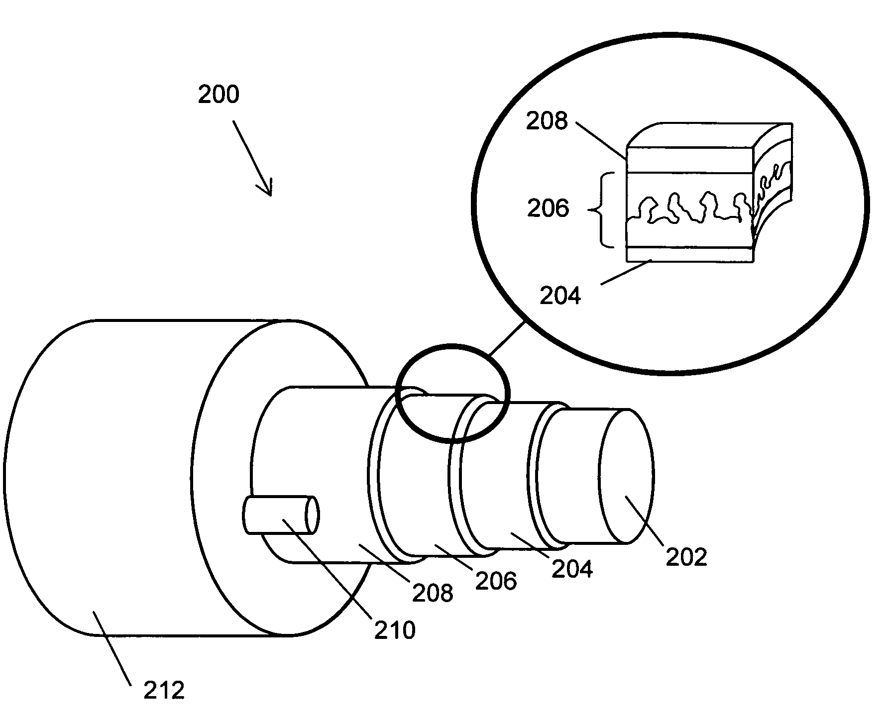
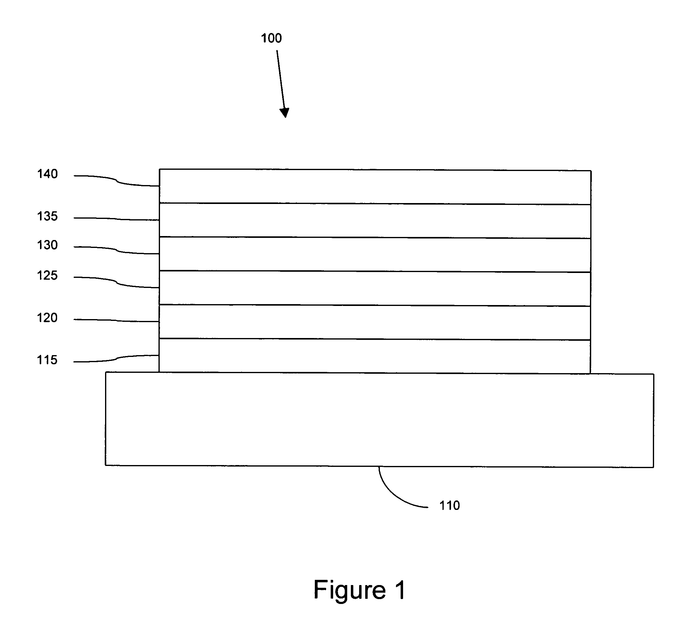
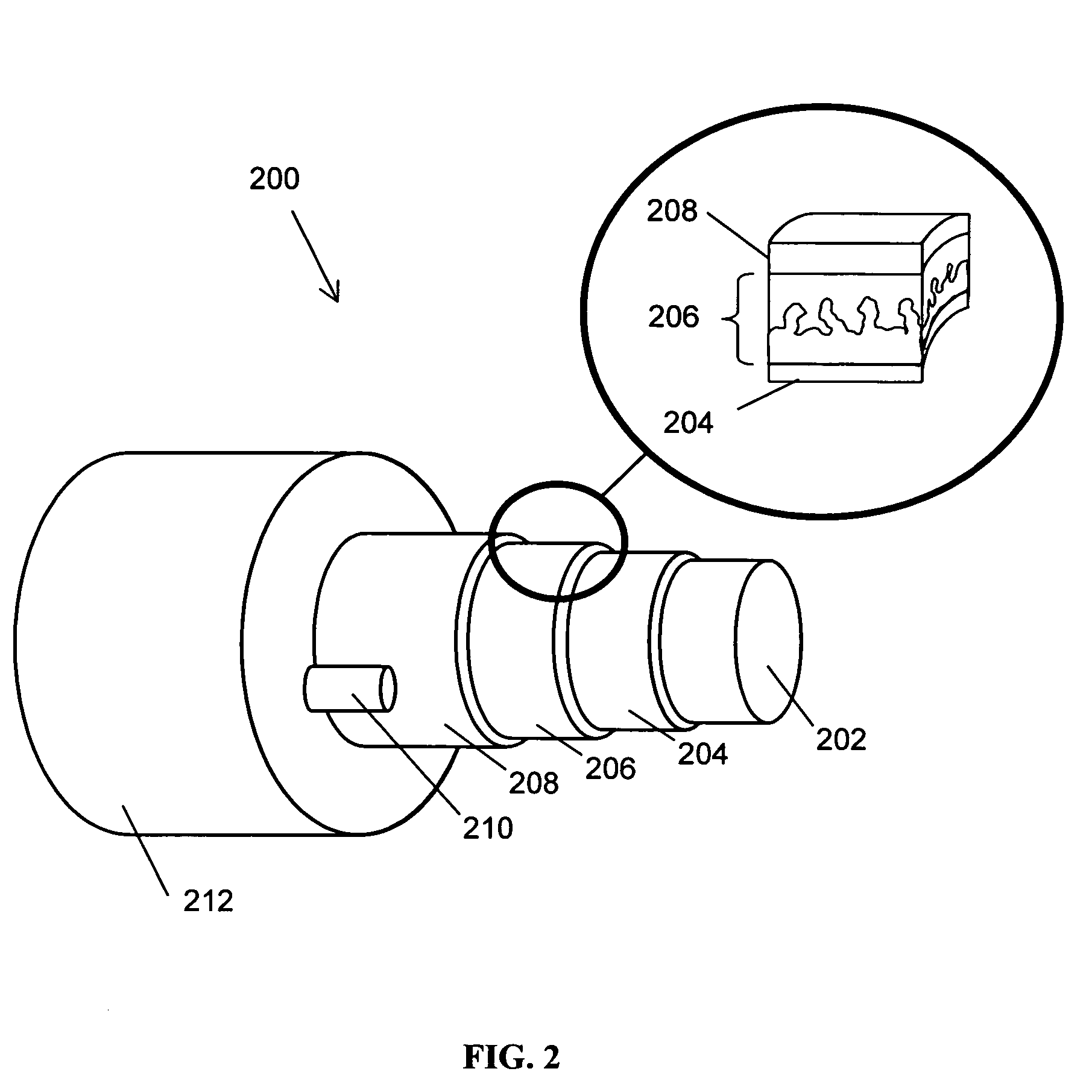
[0031]An organic optoelectronic device is provided, having a fiber structure. Various types of organic optoelectronic devices may be provided, including organic photosensitive devices and organic light emitting devices. Embodiments of the present invention may comprise an anode, a cathode, and an organic layer disposed between and electrically connected to the anode and the cathode.

[0032]Organic photosensitive devices of embodiments of the present invention may be used, for example, to generate a usable electrical current from incident electromagnetic radiation (e.g., PV devices) or may be used to detect incident electromagnetic radiation. A “photoactive region” is the portion of the photosensitive device that absorbs electromagnetic radiation to generate excitons that may dissociate in order to generate an electrical current. Organic photosensitive optoelectronic devices may include at least one transparent electrode to allow incident radiation to be absorbed by the device. Several...


PUM


Abstract

A photoactive fiber is provided, as well as a method of fabricating such a fiber. The fiber has a conductive core including a first electrode. An organic layer surrounds and is electrically connected to the first electrode. A transparent second electrode surrounds and is electrically connected to the organic layer. Other layers, such as blocking layers or smoothing layers, may also be incorporated into the fiber. The fiber may be woven into a cloth.

Description

JOINT RESEARCH AGREEMENT[0001]The claimed invention was made by, on behalf of, and / or in connection with one or more of the following parties to a joint university-corporation research agreement: Princeton University, The University of Southern California, and Global Photonic Energy Corporation. The agreement was in effect on and before the date the claimed invention was made, and the claimed invention was made as a result of activities undertaken within the scope of the agreement.FIELD OF THE INVENTION[0002]The present invention generally relates to organic optoelectronic devices. More specifically, it is directed to organic optoelectronic devices having a fiber structure.BACKGROUND OF THE INVENTION[0003]Optoelectronic devices that make use of organic materials are becoming increasingly desirable for a number of reasons. Many of the materials used to make such devices are relatively inexpensive, so organic opto-electronic devices have the potential for cost advantages over inorgani...

Claims


Application Information

Patent Timeline
Patent Type & Authority Patents(United States)
IPC IPC(8): G02B6/02
CPCH01L51/4206H01L51/424H01L51/5287H01L51/44H01L51/4253H01L27/304H01L27/32H01L51/5012Y02E10/549Y02P70/50H10K30/53H10K59/00H10K30/451H10K30/20H10K30/80H10K30/30H10K50/11H10K50/182H10K99/00
Inventor SHTEIN, MAXFORREST, STEPHEN R.
Owner THE TRUSTEES FOR PRINCETON UNIV
Why Eureka
Try Eureka