Metal-insulator-metal capacitors

a metal-insulator and capacitor technology, applied in capacitors, radiation controlled devices, semiconductor devices, etc., can solve the problems of limiting the applicability of high-speed applications and small designs, not cost competitive, and easy damage to the dielectric layer b>120/b>,

Active Publication Date: 2007-03-27
TAIWAN SEMICON MFG CO LTD
View PDF18 Cites 45 Cited by
  • Summary
  • Abstract
  • Description
  • Claims
  • Application Information

AI Technical Summary

Problems solved by technology

Many times, however, memory chips incorporating other functions and technologies require additional processing steps to incorporate the other functions on a single chip and, thus, are not cost competitive as compared to the alternative of combining separate chips at the card or package level wherein each is being produced with independently optimized technologies.
Furthermore, the dielectric layer 120 may easily become damaged during the etching process to form the top electrode 122 and spacers.
PIP capacitors formed in this manner are typically characterized by lower capacitance and lower conductance, which limits its applicability in high-speed applications and smaller designs.
Additionally, the process is not easily integrated with a high-K dielectric required for a high capacitance design.
The dielectric layer is also easily damaged during the etching process used to form the top electrode.

Method used


Image

  • Metal-insulator-metal capacitors
  • Metal-insulator-metal capacitors
  • Metal-insulator-metal capacitors

Examples


Embodiment Construction

[0016]The making and using of the presently preferred embodiments are discussed in detail below. It should be appreciated, however, that embodiments of the present invention provide many applicable inventive concepts that can be embodied in a wide variety of specific contexts. The specific embodiments discussed are merely illustrative of specific ways to make and use the invention, and do not limit the scope of the invention.

[0017]The present invention will be described with respect to preferred embodiments in a specific context, namely an integrated capacitor compatible with standard semiconductor processing techniques used to fabricate DRAMs. The invention may also be applied, however, to other designs in which it is desirable to integrate capacitors with other semiconductor devices and designs such as signal processing and system-on-chip applications.

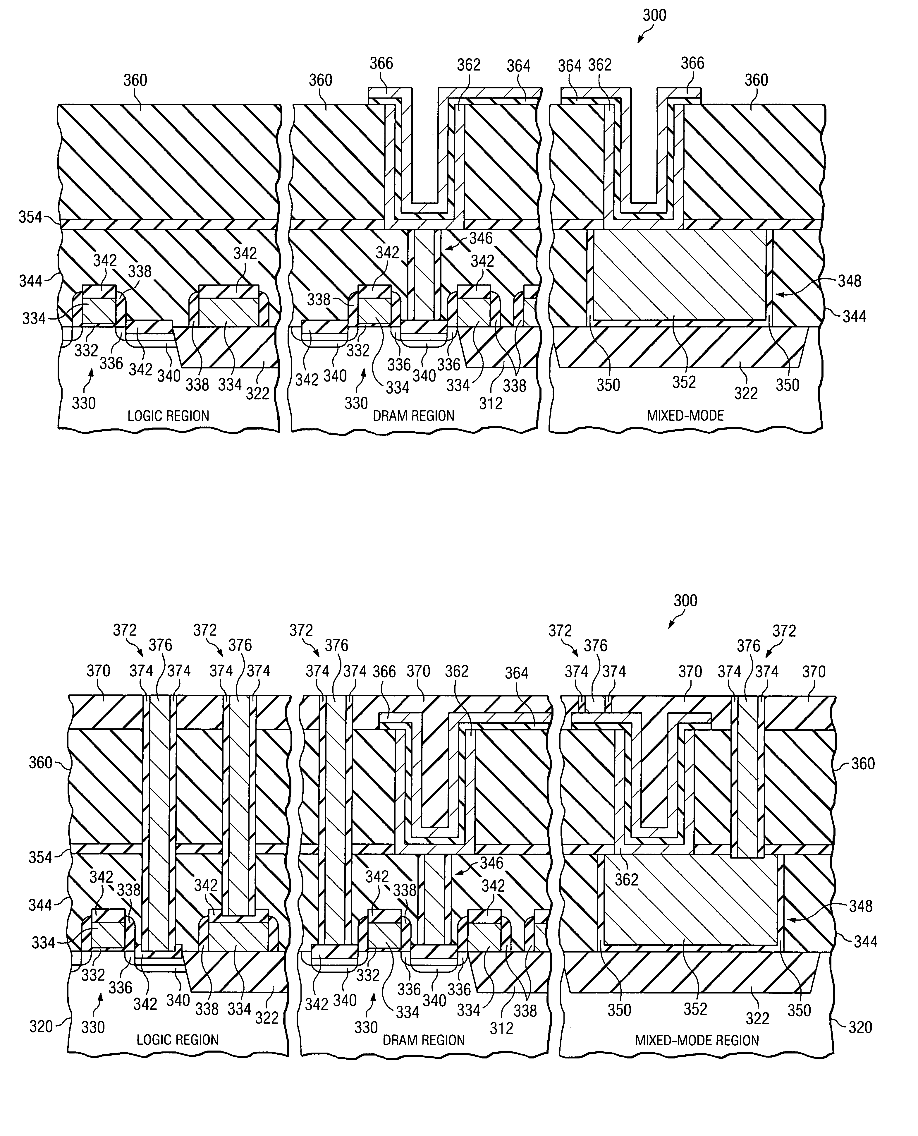
[0018]FIGS. 3a–3g illustrate cross-section views of a wafer 300 during various steps of one embodiment of the present invention in ...


PUM


Abstract

A metal-insulator-metal (MIM) capacitor is provided. The bottom electrode of the MIM capacitor is electrically connected to a connection node. The connection node may be, for example, a contact formed in an interlayer dielectric, a polysilicon connection node, a doped polysilicon or silicon region, or the like. A contact provides an electrical connection between the connection node and components formed above the connection node. A second contact provides an electrical connection to the top electrode.

Description

TECHNICAL FIELD[0001]The present invention relates to the field of semiconductor devices, and more specifically, to semiconductor devices having a metal-insulator-metal capacitor.BACKGROUND[0002]With the increasing array density of successive generations of memory chips, it is desirable to incorporate and merge other functions, and thus other devices, onto the memory chips. Many times, however, memory chips incorporating other functions and technologies require additional processing steps to incorporate the other functions on a single chip and, thus, are not cost competitive as compared to the alternative of combining separate chips at the card or package level wherein each is being produced with independently optimized technologies.[0003]For example, mixed-mode signal processing, radio-frequency (RF) signal processing, and system-on-chip (SoC) semiconductor applications often involve integrating capacitors on memory chips. Integrating capacitors onto chips with other semiconductor ...

Claims


Application Information

Patent Timeline
Patent Type & Authority Patents(United States)
IPC IPC(8): H01L27/148H01L21/02H01L21/8242H01L27/108
CPCH01L28/91H01L27/10894H01L27/10811H01L27/10852H01L28/55H01L28/65H10B12/312H10B12/033H10B12/09
Inventor TU, KUO-CHILIEN, WAI-YI
Owner TAIWAN SEMICON MFG CO LTD
Why Eureka
Try Eureka