Optical element, lithographic apparatus including such an optical element, device manufacturing method, and device manufactured thereby

a technology of optical elements and lithographic apparatuses, applied in the direction of optical radiation measurement, cathode ray tubes/electron beam tubes, photomechanical treatment, etc., can solve the problems of difficult production of gratings and harmful ultraviolet radiation, and achieve good heat conductivity, improve anti-reflection properties of optical elements, and low thermal expansion coefficient

Active Publication Date: 2007-03-27
ASML NETHERLANDS BV
View PDF41 Cites 16 Cited by
  • Summary
  • Abstract
  • Description
  • Claims
  • Application Information

AI Technical Summary

Benefits of technology

[0007]According to an embodiment of the present invention, an optical element includes an anti-reflection coating, wherein the anti-reflection coating is configured to reflect EUV radiation and thereby improve the spectral purity of a radiation beam.
[0027]According to a further embodiment of the present invention, a device is manufactured according to a method including providing a radiation beam; patterning the radiation beam; projecting the patterned beam of radiation onto a substrate; and reflecting the radiation beam with at least one optical element configured to reflect EUV radiation and thereby improve the spectral purity of the radiation beam.

Problems solved by technology

This non-EUV radiation may be harmful for the EUV lithography system, so it should be removed by a spectral purity filter.
These gratings may be difficult to produce, since the surface quality of the triangular shaped pattern has to be very high.

Method used


Image

  • Optical element, lithographic apparatus including such an optical element, device manufacturing method, and device manufactured thereby
  • Optical element, lithographic apparatus including such an optical element, device manufacturing method, and device manufactured thereby
  • Optical element, lithographic apparatus including such an optical element, device manufacturing method, and device manufactured thereby

Examples


Embodiment Construction

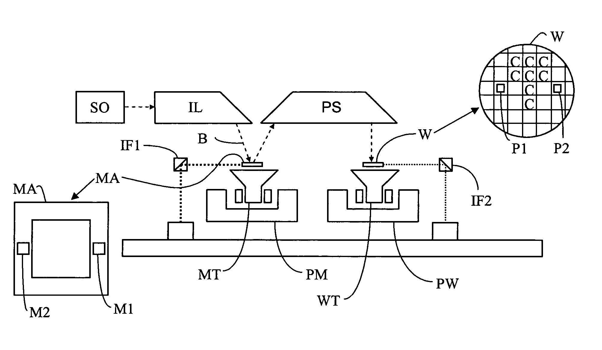
[0041]FIG. 1 schematically depicts a lithographic apparatus according to one embodiment of the invention. The apparatus includes an illumination system (illuminator) IL configured to condition a radiation beam B (e.g. UV radiation or EW radiation). A support (e.g. a mask table) MT is configured to support a patterning device (e.g. a mask) MA and is connected to a first positioning device PM configured to accurately position the patterning device in accordance with certain parameters. A substrate table (e.g. a wafer table) WT is configured to hold a substrate (e.g. a resist-coated wafer) W and is connected to a second positioning device PW configured to accurately position the substrate in accordance with certain parameters. A projection system (e.g. a refractive projection lens system) PS is configured to project a pattern imparted to the radiation beam B by patterning device MA onto a target portion C (e.g. including one or more dies) of the substrate W.

[0042]The illumination syste...


PUM

PropertyMeasurementUnit
thickaaaaaaaaaa
angles of incidenceaaaaaaaaaa
thicknessaaaaaaaaaa

Abstract

An optical element including an anti-reflection (AR) coating is configured to reflect Extreme-Ultra-Violet (EUV) radiation only.

Description

BACKGROUND OF THE INVENTION[0001]1. Field of the Invention[0002]The present invention relates to an optical element, a lithographic apparatus including such an optical element, a device manufacturing method, and a device manufactured thereby.[0003]2. Description of the Related Art[0004]A lithographic apparatus is a machine that applies a desired pattern onto a substrate, usually onto a target portion of the substrate. A lithographic apparatus can be used, for example, in the manufacture of integrated circuits (ICs). In that instance, a patterning device, which is alternatively referred to as a mask or a reticle, may be used to generate a circuit pattern to be formed on an individual layer of the IC. This pattern can be transferred onto a target portion (e.g. including part of, one, or several dies) on a substrate (e.g. a silicon wafer). Transfer of the pattern is typically via imaging onto a layer of radiation-sensitive material (resist) provided on the substrate. In general, a sing...

Claims


Application Information

Patent Timeline
Patent Type & Authority Patents(United States)
IPC IPC(8): G03F7/20G02B27/14
CPCG03F7/70575G21K1/06G03F7/70958G21K2201/067G02B1/113G02B5/0891
Inventor VAN HERPEN, MAARTEN MARINUS JOHANNES WILHELMUSBAKKER, LEVINUS PIETERKLUNDER, DERK JAN WILFRED
Owner ASML NETHERLANDS BV
Why Eureka
Try Eureka