

Semiconductor device including a high voltage transistor
a high-voltage transistor and semiconductor technology, applied in the direction of semiconductor devices, basic electric elements, electrical appliances, etc., can solve the problems of difficult control of impurity concentration, easy lowering of electric current driving capability of high-voltage transistors, and difficulty in controlling electric current driving capability. , to achieve the effect of suppressing the reduction of the electric current driving capability of the transistor, easy control, and high withstand voltag
- Summary
- Abstract
- Description
- Claims
- Application Information
AI Technical Summary
Benefits of technology
Problems solved by technology
Method used
Image

Examples
embodiment 1
[0031
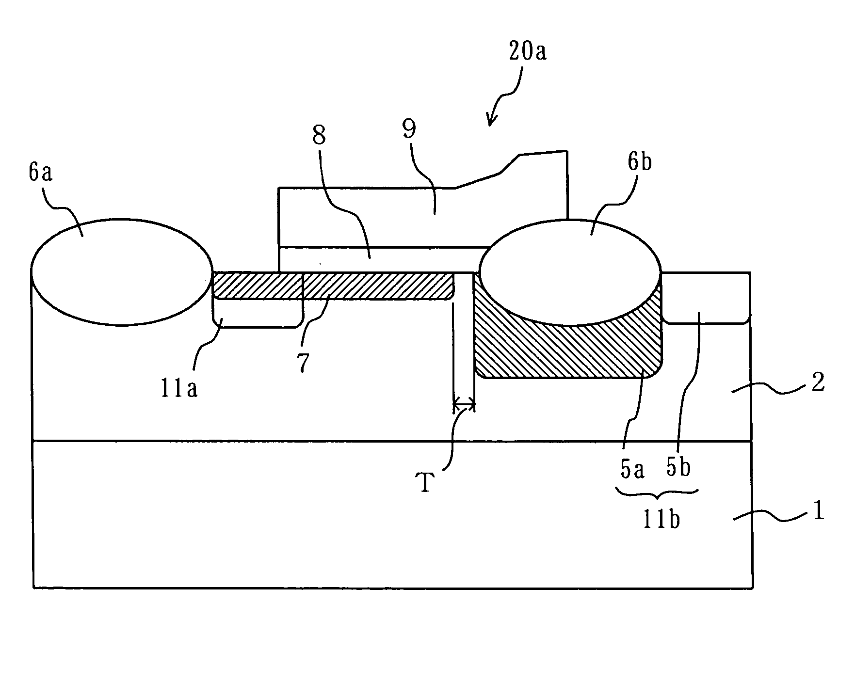
[0032]FIG. 1 is a cross-sectional view of a structure of a semiconductor device according to Embodiment 1 of the present invention, including a MOS type transistor processed with device isolation by LOCOS and having an offset structure. In FIG. 1, a semiconductor substrate has a first conductivity type impurity surface portion. Here, the semiconductor substrate includes a semiconductor base 1 used as a base for forming a high voltage transistor 20a, and a first conductivity type well diffusion layer 2 formed thereon. On a surface of the well diffusion layer 2, LOCOS oxide films 6a and 6b are formed as insulating films for device isolation.
[0033]A second conductivity type source diffusion layer 11a is formed in the well diffusion layer 2 so as to contact the LOCOS oxide film 6a. A second conductivity type drain diffusion layer 11b includes a low impurity concentration region 5a and a high impurity concentration region 5b. The low impurity concentration region 5a is located on th...
embodiment 2
[0050
[0051]In this embodiment, a semiconductor device including a border impurity layer provided between the low impurity concentration region 5a and the impurity layer 7 will be described. The semiconductor device according to this embodiment has substantially the same structure as that of the semiconductor device according to Embodiment 1, and only differences will be described below.
[0052]FIG. 4 is a cross-sectional view of a structure of a semiconductor device according to Embodiment 2 of the present invention. In FIG. 4, a second conductivity type border impurity layer 10 is provided between the low impurity concentration region 5a and the impurity layer 7.
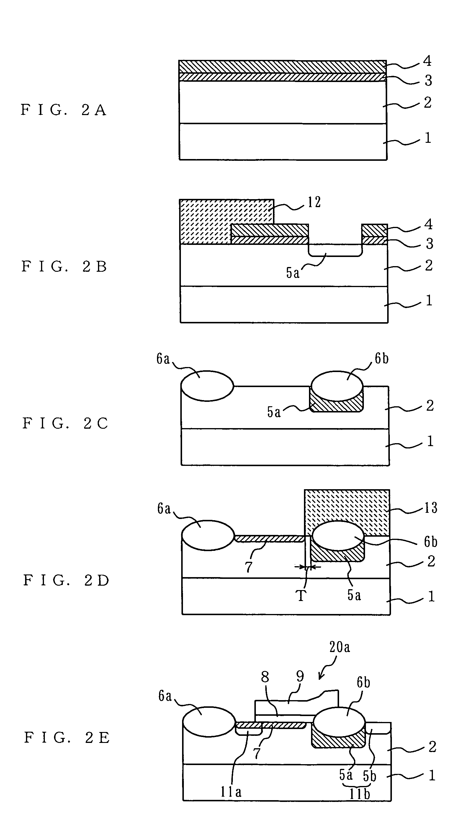
[0053]FIGS. 5A through 5E are cross-sectional views of a semiconductor substrate and elements formed thereon in steps of fabrication of the semiconductor device shown in FIG. 4. Hereinafter, with reference to FIGS. 5A through 5E, a method for fabricating the semiconductor device according to Embodiment 2 will be described. Th...
PUM
 Abstract
Description
Claims
Application Information