Direct conversion receiver with direct current offset correction circuitry

a technology of offset correction and direct conversion circuit, which is applied in the field of analog integrated circuit design, can solve the problems of limiting the practical implementation of the direct conversion circuit, the greater the chance of irreversible data loss, and the greater the decay of the signal, so as to achieve less noise 1/f

Active Publication Date: 2007-03-27
SEMICON COMPONENTS IND LLC
View PDF46 Cites 12 Cited by
  • Summary
  • Abstract
  • Description
  • Claims
  • Application Information

AI Technical Summary

Benefits of technology

[0013]The foregoing problems with the prior state of the art are overcome by the principles of the present invention, which are directed towards a direct conversion circuit that includes an in-phase and quadrature-phase feedback path that reduces Direct Current (DC) offset. Each feedback path includes a compensating mixer that generates an error correction voltage that is passed through a loop gain circuit and an integrator. The integrated signal is applied to the output of a low pass filter that operates on the down-converted baseband signal. The direction conversion circuit may not only down convert the received modulated signal using a down-converting mixer into a baseband signal, but also, after performing a passive low pass filtering to remove higher-order components, performs up-conversion of the baseband signal using an up-converting mixer. This allows active elements operating on the up-converted signal to introduce less 1 / f noise.

Problems solved by technology

The further a signal is transmitted, however, the greater the decay in the signal and the greater the chance for irreversible loss in the data represented by the signal.
However, there are some performance issues for the direct conversion circuit of FIG. 5 that limit its practical implementation.
In particular, conventional direct conversion circuits suffer from Direct Current (DC) offset.
Such DC offsets can swamp out the much weaker desired signal.
However, as mentioned above, many direct conversion circuits also have some drawbacks in the form of increased DC offset.

Method used


Image

  • Direct conversion receiver with direct current offset correction circuitry
  • Direct conversion receiver with direct current offset correction circuitry
  • Direct conversion receiver with direct current offset correction circuitry

Examples


Embodiment Construction

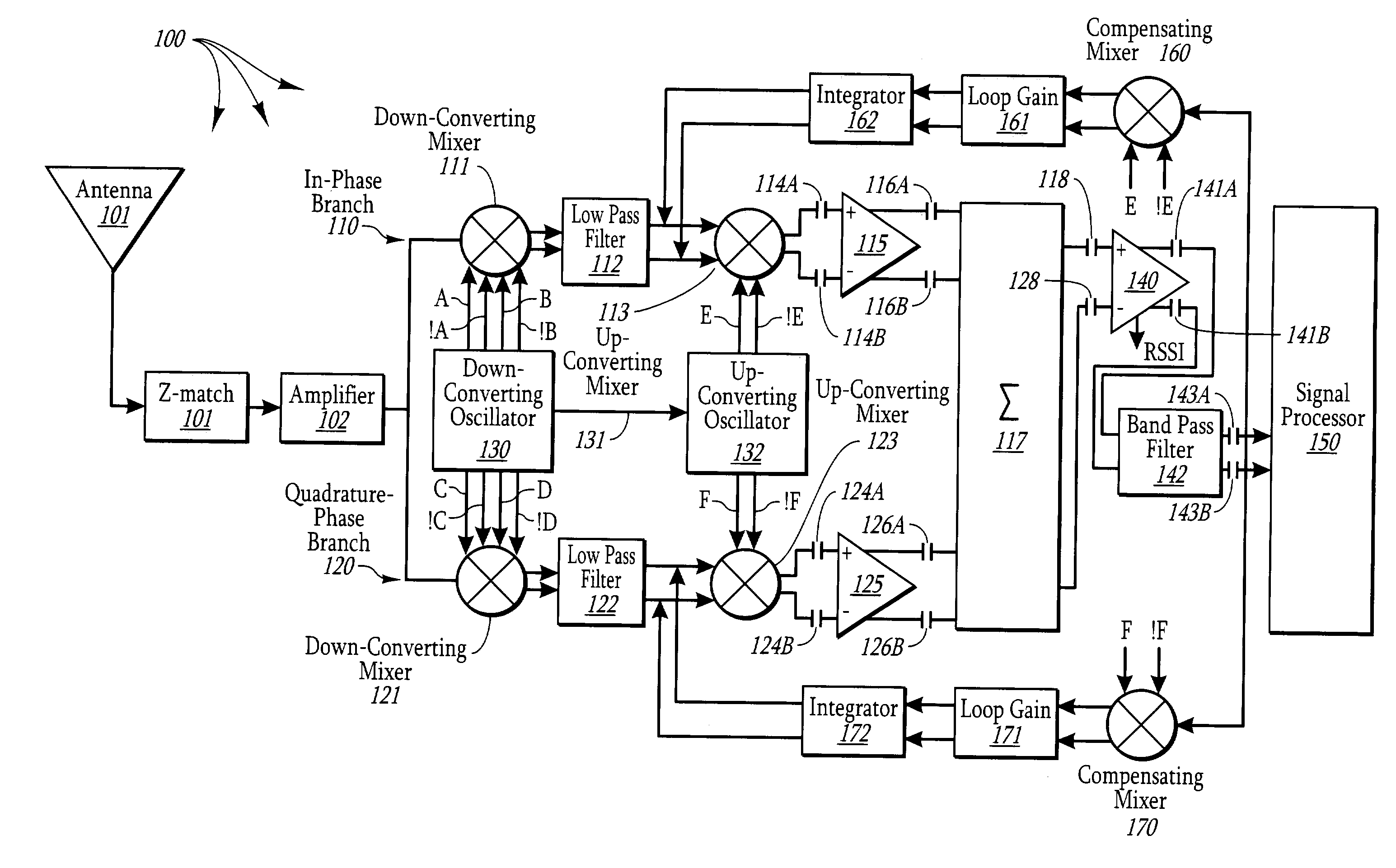
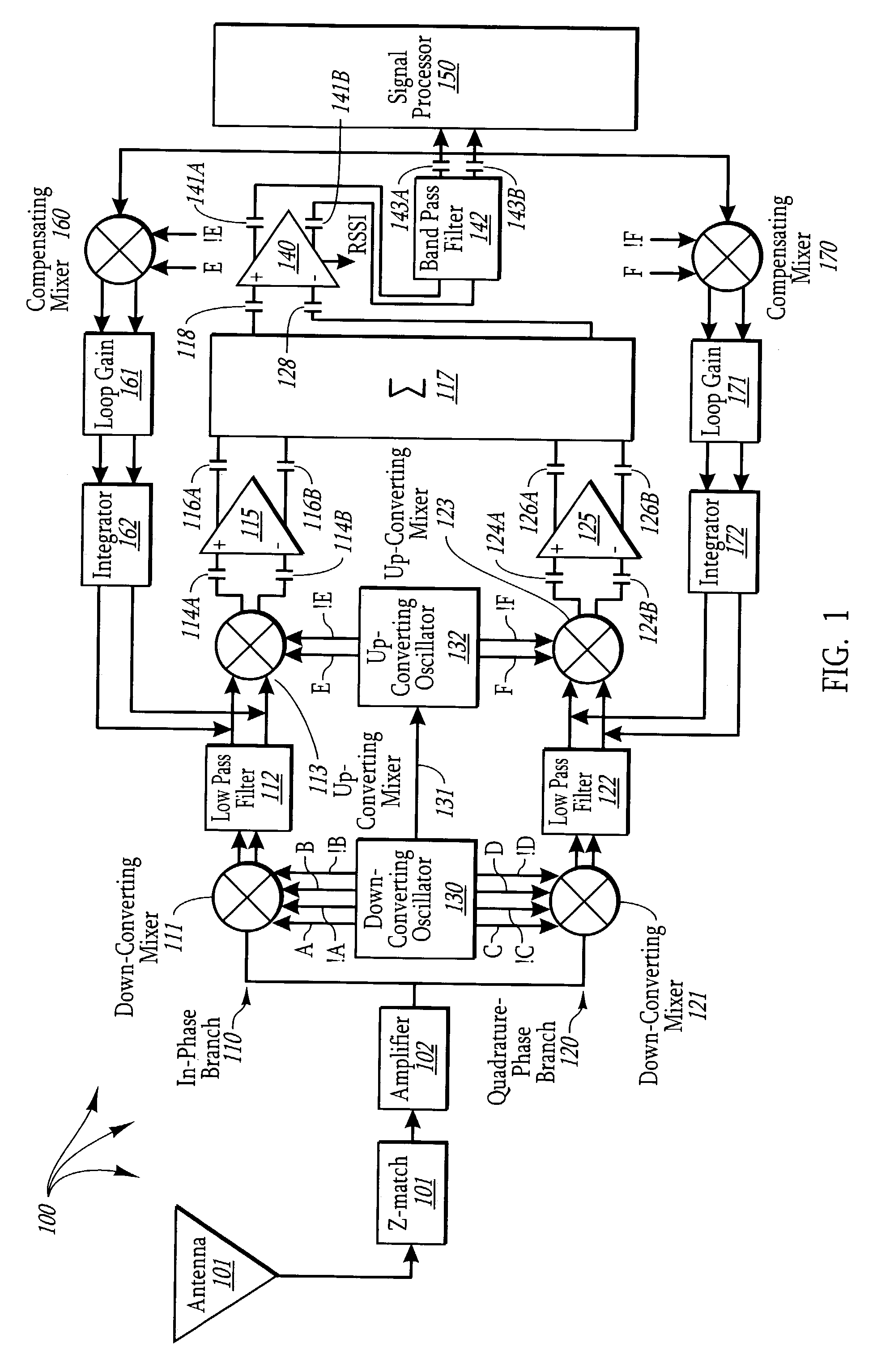
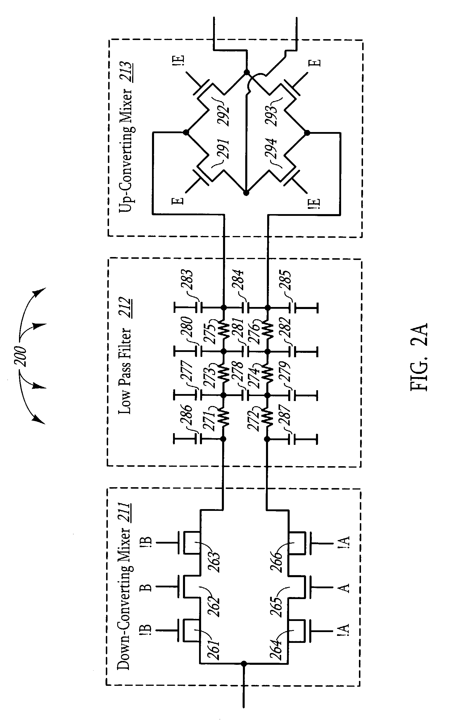
[0023]The principles of the present invention are directed towards a direct conversion circuit that includes a compensating mixer that feeds back into the output terminals of the low pass filter that follows the down-converting mixer to thereby at least partially compensate for Direct Current (DC) offset. DC offset and also 1 / f noise may be reduced further by including an up-converting mixer following the down-converting mixer.

[0024]In this description and in the claims, one node in a circuit is “coupled” to another node in the circuit if charge carriers freely flow (even through some devices and / or with some resistance) between the two nodes during normal operation of the circuit. One node in a circuit is “capacitively coupled” to another node in the circuit if there are one or more capacitors that intervene between the two nodes. One node in a circuit is “at least capacitively coupled” to another node if the two nodes are either coupled together as just defined, or are capacitive ...


PUM


Abstract

A direct conversion circuit that includes an in-phase and quadrature-phase feedback path that reduces Direct Current (DC) offset. Each feedback path includes a compensating mixer that generates an error correction voltage that is passed through a loop gain circuit and an integrator. The integrated signal is applied to the output of a low pass filter that operates on the down-converted baseband signal. The direction conversion circuit may not only down convert the received modulated signal using a down-converting mixer into a baseband signal, but also, after performing a passive low pass filtering to remove higher-order components, performs up-conversion of the baseband signal using an up-converting mixer. This allows active elements operating on the up-converted signal to introduce less 1/f noise.

Description

BACKGROUND OF THE INVENTION[0001]1. The Field of the Invention[0002]The present invention relates to analog integrated circuit design, and more particularly, to direct conversion receivers having reduced Direct Current (DC) offset.[0003]2. Background and Related Art[0004]Electrical signals have proven to be an effective means of conveying data from one location to another. The further a signal is transmitted, however, the greater the decay in the signal and the greater the chance for irreversible loss in the data represented by the signal. In order to guard against this signal decay, the core electrical signal that represents the data (i.e., the baseband signal) may be modulated or superimposed on a carrier wave in the Radio Frequency (RF) frequency spectrum.[0005]In order to properly interpret the signal, conventional RF receivers extracts the baseband signal from the received signal. The data represented by the extracted baseband signal may then be interpreted by other downstream ...

Claims


Application Information

Patent Timeline
Patent Type & Authority Patents(United States)
IPC IPC(8): H03D3/22H04L27/22
CPCH03D3/007
Inventor PETROV, ANDREI R.CHRISTENSEN, CRAIG L.
Owner SEMICON COMPONENTS IND LLC
Why Eureka
Try Eureka