Compositions, methods for producing films, functional elements, methods for producing functional elements, method for producing electro-optical devices and methods for producing electronic apparatus

Inactive Publication Date: 2007-04-03
SEIKO EPSON CORP
View PDF30 Cites 46 Cited by
  • Summary
  • Abstract
  • Description
  • Claims
  • Application Information

AI Technical Summary

Benefits of technology

[0043]The solvent may be a single solvent including one of the heterocyclic compounds, or a mixed solvent including two types or more of the heterocyclic compounds. Alternatively, the solvent may be a mixture including the heterocyclic compound and another solvent other than the heterocyclic compound. Benzene derivatives are preferred as the solvent other than the heterocyclic compound. Examples of such benzene derivatives are cymene, tetralin, cumene, decalin, durene, cyclohexylbenzene, dihexylbenzenes, tetramethylbenzenes and dibutylbenzenes. By using these solvents, the composition can have a controlled viscosity that is appropriate for the application, and the target functional film can easily be designe

Problems solved by technology

However, the photolithography process is subject to disadvantages, such

Method used


Image

  • Compositions, methods for producing films, functional elements, methods for producing functional elements, method for producing electro-optical devices and methods for producing electronic apparatus
  • Compositions, methods for producing films, functional elements, methods for producing functional elements, method for producing electro-optical devices and methods for producing electronic apparatus
  • Compositions, methods for producing films, functional elements, methods for producing functional elements, method for producing electro-optical devices and methods for producing electronic apparatus

Examples


example 1

[0063]A composition (G1) (solution) indicated in Table 1 was prepared as a composition for a green light-emitting layer.

[0064]A composition (B1) (solution) indicated in Table 2 was prepared as a composition for a blue light-emitting layer.

[0065]A composition (R1) (solution) indicated in Table 3 was prepared as a composition for a red light-emitting layer.

[0066]

TABLE 1Light-emitting Layer (Green) CompositionCompositionMaterialCompositional AmountLight-emitting layerCompound 10.76gmaterialCompound 20.20gCompound 30.04gSolvent2,3-Dihydrobenzofuran60mlCyclohexylbenzene40ml

[0067]

TABLE 2Light-emitting Layer (Blue) CompositionCompositionMaterialCompositional AmountLight-emitting layerCompound 10.78gmaterialCompound 20.25gCompound 40.07gSolvent2,3-Dihydrobenzofuran60mlCyclohexylbenzene40ml

[0068]

TABLE 3Light-emitting Layer (Red) CompositionCompositionMaterialCompositional AmountLight-emitting layerCompound 10.70gmaterialCompound 20.20gCompound 50.10gSolvent2,3-Dihydrobenzofuran60mlCyclohexyl...

example 2

[0076]A hole injection-transportation composition (solution) having a formula shown in Table 5 below was prepared.

[0077]

TABLE 5Hole Injection-transportation CompositionCompositionMaterial NameContent (wt. %)Hole injection-Baytron P11.08transportation materialPoly(styrene Sulfonate)1.44Polar solventIsopropyl alcohol10N-Methylpyrrolidone27.481,3-Dimethyl-imidazolinone50

[0078]The composition (solution) shown in Table 1 was prepared as a green light-emitting layer composition.

[0079]Next, a method for producing an organic EL element by the ink-jet process using these materials will be illustrated. In advance of this, a schematic configuration of an example of an organic EL panel will be illustrated as an electro-optical device using the organic EL element as a functional element.

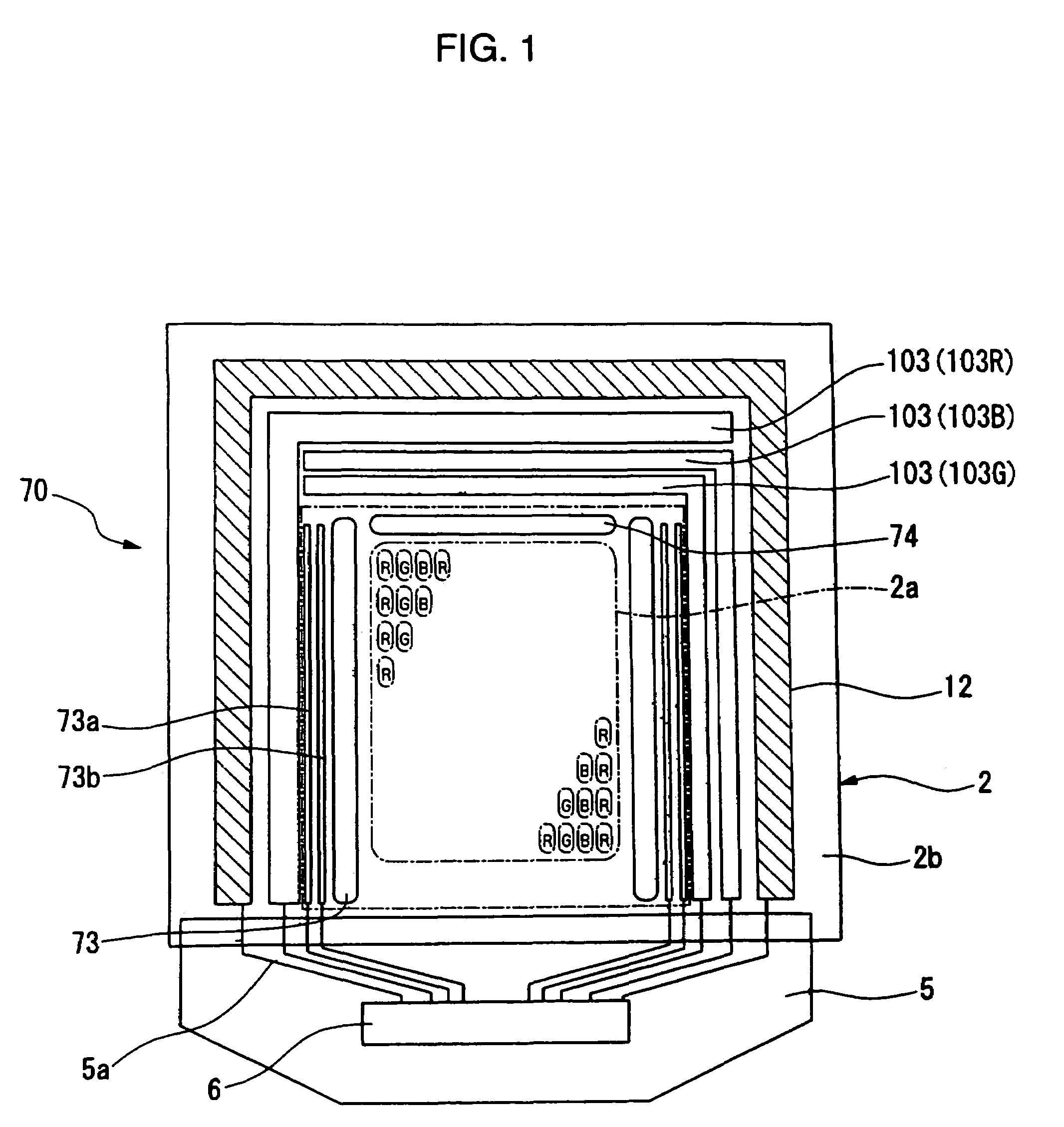
[0080]FIG. 1 is a schematic of a planar structure of an example of such an organic EL panel as an electro-optical device, in which the reference numeral 70 is an organic EL panel. The organic EL panel 70 includes...

example 3

[0099]A substrate having a multilayer structure including an ITO electrode, a SiO film and a polyimide film, each having a predetermined shape of an opening, was prepared, and a hole injection-transportation layer was applied thereto in the same manner as in Example 2. Next, a green light-emitting layer composition (having the formula shown in Table 1) was then applied onto the substrate, and immediately after the application, the substrate was heated at 60° C., while the solvent under a reduced pressure (2 mm-Hg) was removed, and thereby a green light-emitting layer was yielded. Subsequently, an element (3) was prepared under the same conditions as in Example 2, except for the drying condition, and the voltage-luminance characteristic of the element (3) was measured. The same result as in Example 2 was obtained.


PUM

PropertyMeasurementUnit
Temperatureaaaaaaaaaa
Angleaaaaaaaaaa
Vapor pressureaaaaaaaaaa

Abstract

In accordance with the invention, a composition including a solvent and a functional material is prepared. The solvent includes at least one heterocyclic compound having one or more substituents and containing an oxygen atom as a constituent atom. The functional material is selected from a group including organic EL materials, conductive materials, insulative materials and semiconductive materials. Functional films and functional elements are prepared by using the composition.

Description

[0001]This is a Division of Application No. 10 / 095,048 filed March 12, 2002, now U.S. Pat. No. 6,787,063 issued Sep. 7, 2004. The entire disclosure of the prior application is hereby incorporated by reference herein in its entirety.BACKGROUND OF THE INVENTION[0002]1. Field of Invention[0003]The present invention relates to a composition (a discharge composition) that can be used for the formation of thin films of functional materials, especially for the formation of patterned films of functional materials using discharge devices, and that can stably be discharged. The invention also relates to a method for producing a uniform film (a functional film) using the composition, to a functional element, to a method for producing the functional element, to a method for producing an electro-optical device and to a method for producing electronic apparatus.[0004]2. Description of Related Art[0005]Thin films can be produced from liquid phases by a wide variety of processes, such as by a spin ...

Claims


Application Information

Patent Timeline
IPC IPC(8): B05D5/12H01L51/00H01L51/30H01L51/40H01L51/50
CPCH01L51/0004H01L51/0005H01L51/0007H01L51/0034H01L51/0035H01L51/0036H01L51/0039H01L51/0043H01L51/0053H01L51/0059H01L51/5012H10K71/13H10K71/15H10K71/135H10K85/10H10K85/115H10K85/111H10K85/151H10K85/113H10K85/621H10K85/631H10K50/11
Inventor ENDO, AYAESEKI, SHUNICHIMORII, KATSUYUKI
Owner SEIKO EPSON CORP
Why Eureka
Try Eureka