Device with quantum dot layer spaced from delta doped layer
Inactive Publication Date: 2007-04-03
THE BOARD OF TRUSTEES OF THE UNIV OF ILLINOIS +1
View PDF17 Cites 2 Cited by
Summary
Abstract
Description
Claims
Application Information
AI Technical Summary
This helps you quickly interpret patents by identifying the three key elements:
Problems solved by technology
Method used
Benefits of technology
[0006]A major problem with quantum dot heterostructures (QDHs) is the stochastic nature of QD structures, the lack of uniformity, insufficient QD density, and poor QD-to-QD coupling. In accordance with an aspect hereof, a solution to the problem is to couple, via a thin barrier, the sheet (or multiple sheets) of QDs to an auxiliary layer. In a form hereof, the auxiliary layer is a QW layer, e.g., the QW layer of a QW laser. The higher energy states of the QDs are resonant with and couple by tunneling to the lower confined-particle states of the thin uniform QW layer. Electr
Problems solved by technology
A major problem with quantum dot heterostructures (QDHs) is the stochastic nature of QD
Method used
Image
Click on the blue label to locate the original text in one second.
Reading with bidirectional positioning of images and text.
Examples
Example
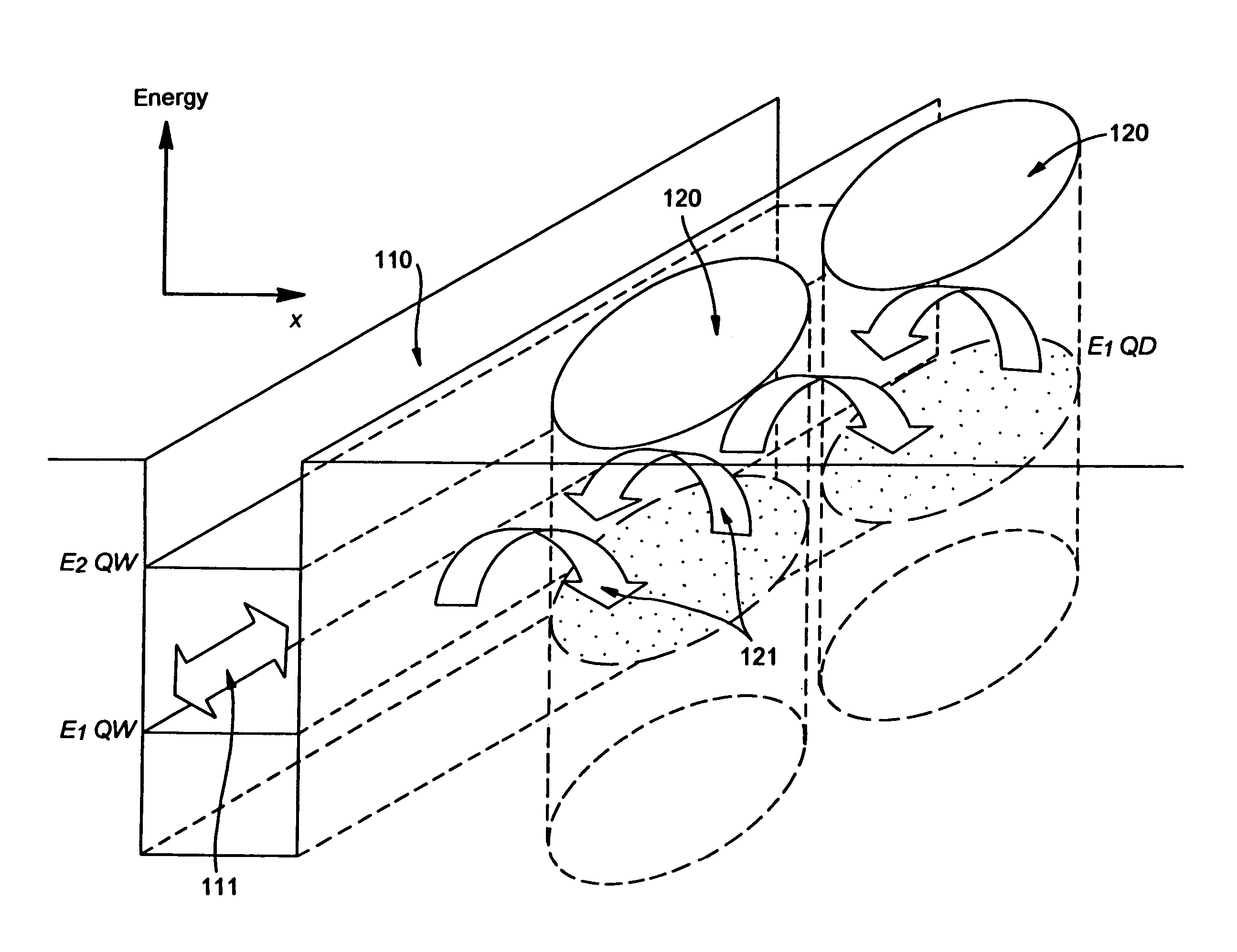
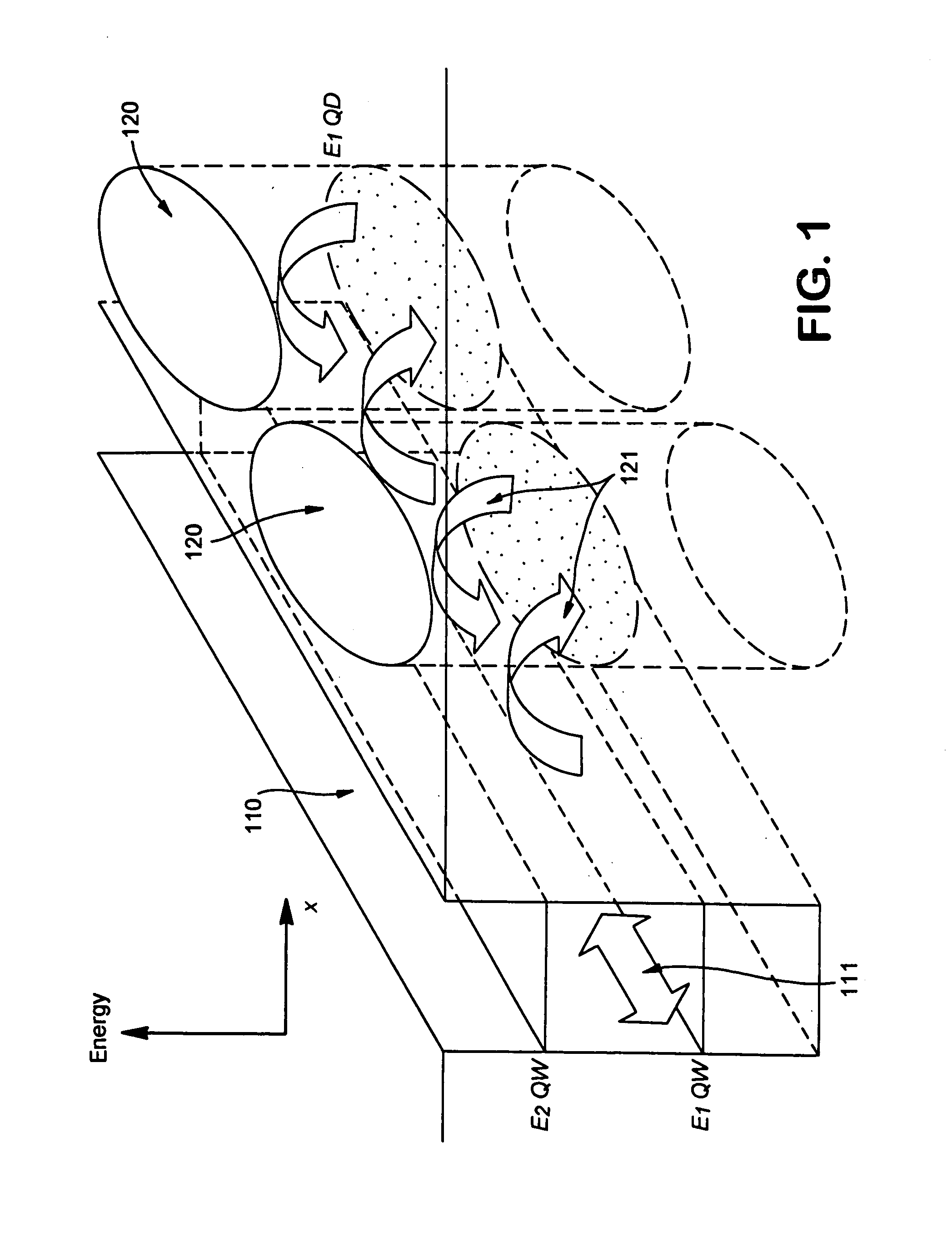
[0034]FIG. 1 is a diagram illustrating intra-QW carrier transport, and inter-QD-QW transport (in both directions) by tunnelling of carriers in a device with a quantum dot layer disposed in close proximity to a quantum well layer. In FIG. 1, the vertical direction represents energy level, and the x direction is normal to the plane of the device layers. The quantum well communication layer is represented at 110, and quantum dots are represented at 120. Quantum well energy states are labelled at E1QW and E2QW, and quantum dot energy state is labelled at E1QD. Double-headed arrow III represents intra QW transport, and the arrows 121 represent inter QW-QD transport in both directions. As seen from the diagram, an electron can, for example, tunnel from quantum dot to the quantum well layer, transports in the quantum well layer, and re-tunnels back into another quantum dot. In this manner, it is possible for the charge to get unstuck from a quantum dot and move from dot to dot in the waveg...
PUM
Abstract
A method of forming a semiconductor device includes the following steps: providing a plurality of semiconductor layers; providing means for coupling signals to and/or from layers of the device; providing a layer of quantum dots disposed between adjacent layers of the device; and providing an auxiliary layer disposed in one of the adjacent layers, and spaced from the layer of quantum dots, the auxiliary layer being operative to communicate carriers with the layer of quantum dots.
Description
RELATED APPLICATION[0001]This is a divisional of U.S. application Ser. No. 10 / 330,692 filed Dec. 27, 2002 now U.S. Pat. No. 6,773,949, which is a continuation-in part of U.S. application Ser. No. 10 / 209,279 filed Jul. 31, 2002 now U.S. Pat. No. 6,753,273, which, in turn, claims priority from U.S. Provisional Application Ser. No. 60 / 309,149, filed Jul. 31, 2001. The said application Ser. No. 10 / 330,692 is hereby incorporated by reference.[0002]This invention was made with Government support, and the Government has certain rights in this inventionFIELD OF THE INVENTION[0003]This invention relates to the field of semiconductor devices and methods of making same, and, more particularly, to a semiconductor device having a layer of quantum dots and at least one other layer, spaced therefrom, which communicates carriers in either direction with the quantum dot layer, and to a method of making such a device.BACKGROUND OF THE INVENTION[0004]In 1977 there was introduced the quantum-well (QW) ...
Claims
Application Information
Patent Timeline
Application Date:The date an application was filed.
Publication Date:The date a patent or application was officially published.
First Publication Date:The earliest publication date of a patent with the same application number.
Issue Date:Publication date of the patent grant document.
PCT Entry Date:The Entry date of PCT National Phase.
Estimated Expiry Date:The statutory expiry date of a patent right according to the Patent Law, and it is the longest term of protection that the patent right can achieve without the termination of the patent right due to other reasons(Term extension factor has been taken into account ).
Invalid Date:Actual expiry date is based on effective date or publication date of legal transaction data of invalid patent.