System for remediating cross contamination in semiconductor manufacturing processes

a technology for cross contamination and manufacturing processes, applied in the field of systems, can solve the problems of reducing device parametric performance, generating numerous challenges to the semiconductor manufacturing process, and reducing device yield, so as to reduce yield loss, reduce cost, and reduce the effect of manufacturing costs

Active Publication Date: 2007-04-03
TEXAS INSTR INC
View PDF3 Cites 7 Cited by
  • Summary
  • Abstract
  • Description
  • Claims
  • Application Information

AI Technical Summary

Benefits of technology

[0012]The present invention provides a versatile system for detecting and remediating cross-contamination, particularly copper cross-contamination, in semiconductor manufacturing processes. The present invention provides a versatile remediation system that operates, in-line, within semiconductor manufacturing equipment and processes—efficiently streamlining cross-contamination testing. With the present invention, semiconductor wafers are inspected for cross-contamination in a non-invasive, non-destructive manner—eliminating any yield loss due solely to testing. The remediation system of the present invention also provides specific indication of cross-contamination location(s), which provides the ability to quickly identify and remediate the origin(s) or source(s) of cross-contamination. The present invention thus provides timely, non-destructive remediation of semiconductor cross-contamination in an easy, efficient and cost-effective manner.
[0013]The system of the present invention is readily implemented within high-volume semiconductor manufacturing processes, without substantial imposition on existing process flows or fabrication systems. A system according to the present invention may be implemented as a stand-alone system inserted into a manufacturing process, or may be implemented as an integrated component or module of an already-existing system within the manufacturing process. Specifically, the present invention provides a measurement system, an activation system, and an analytical system. Electrical behavior profiles of a suspect wafer are measured, before and after exposure to an activating source, and then analyzed to determine if and where contamination may be present. Specific results are provided, graphically or otherwise, in a matter of minutes—enabling timely efficient decontamination of a tool or system from which the wafer emerged.

Problems solved by technology

The increased packing density of the integrated circuit generates numerous challenges to the semiconductor manufacturing process.
Performance advantages provided by such materials, however, have not come without cost.
Certain physical and behavioral properties of these alternative materials can cause of number of problems during the manufacture, testing or operation of a semiconductor.
Copper contamination of non-cupric semiconductor materials can significantly degrade device parametric performance, or cause complete device failure altogether.
This naturally results in a number of yield and reliability problems.
Cross-contamination can occur in or at a number of processing systems or stations (e.g., device inspection, cleaning chambers), since such systems must be used to process multiple devices at various stages throughout the front-end and back-end processes.
For many manufacturers, it is not economically feasible or efficient to employ separate, redundant equipment for front-end / back-end materials and processes, solely for the sake of avoiding cross-contamination.
Often, therefore, potentially harmful cross-contamination is mitigated by other means.
There are, however, a number of issues that typically arise in conventional copper contamination inspection methods and systems.
One issue concerns the frequency of inspections conducted.
Furthermore, each of the semiconductor wafers processed by that system or tool, since its last satisfactory inspection, must either be scrapped or individually inspected.
Either way, time and money are wasted and lost.
This introduces a certain degree of inefficiency into the production process.
Many conventional inspection systems and methods are also rather time-consuming—often taking an hour or more to provide a complete analysis.
Besides further increasing inefficiency of the process, a long inspection time allows for a large number of wafers to be processed by a potentially contaminated system or tool.
Moreover, many conventional copper contamination detection systems and methods provide little, if any, indication of the specific position or source of copper contamination within a particular processing system or tool.

Method used


Image

  • System for remediating cross contamination in semiconductor manufacturing processes
  • System for remediating cross contamination in semiconductor manufacturing processes

Examples


Embodiment Construction

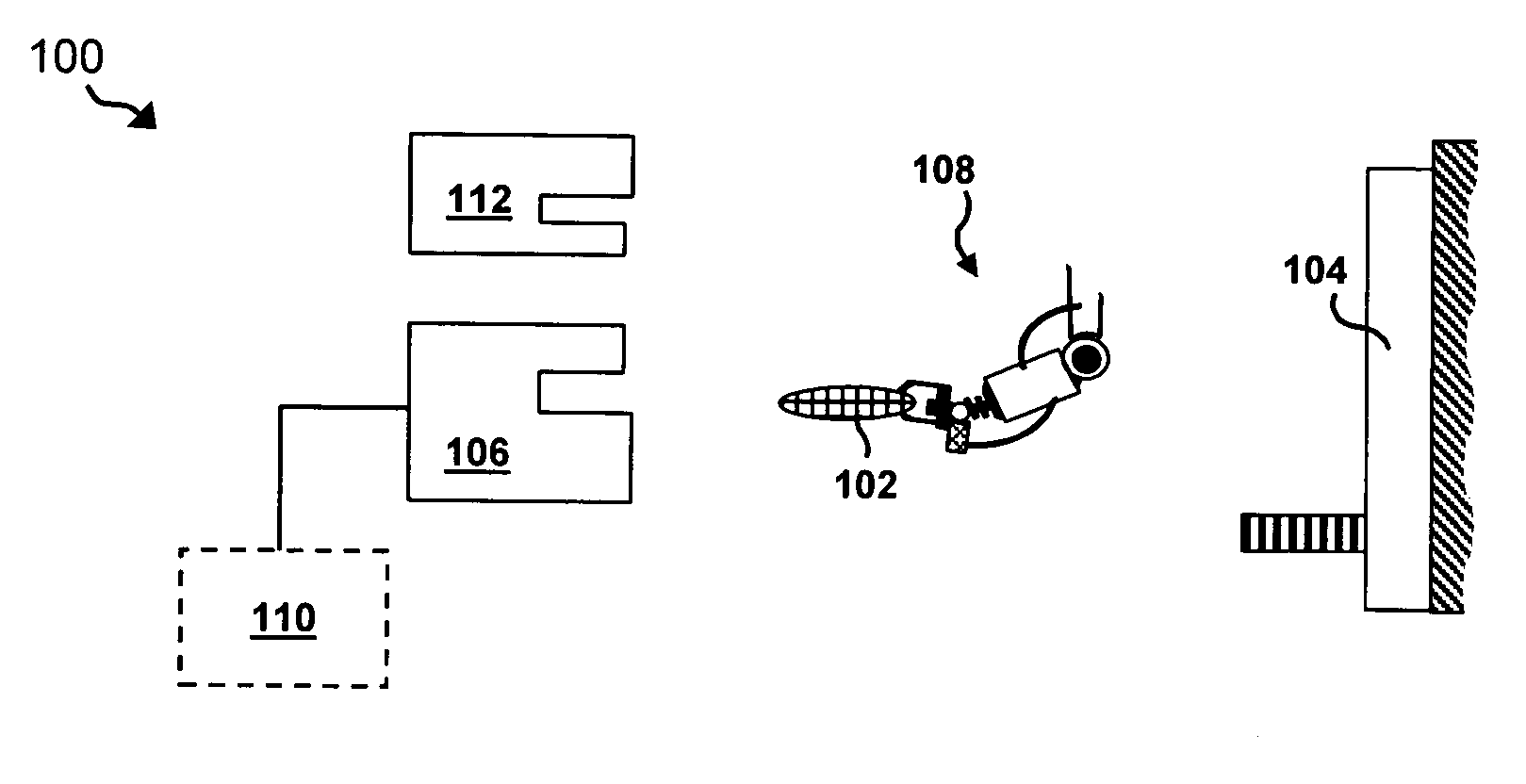
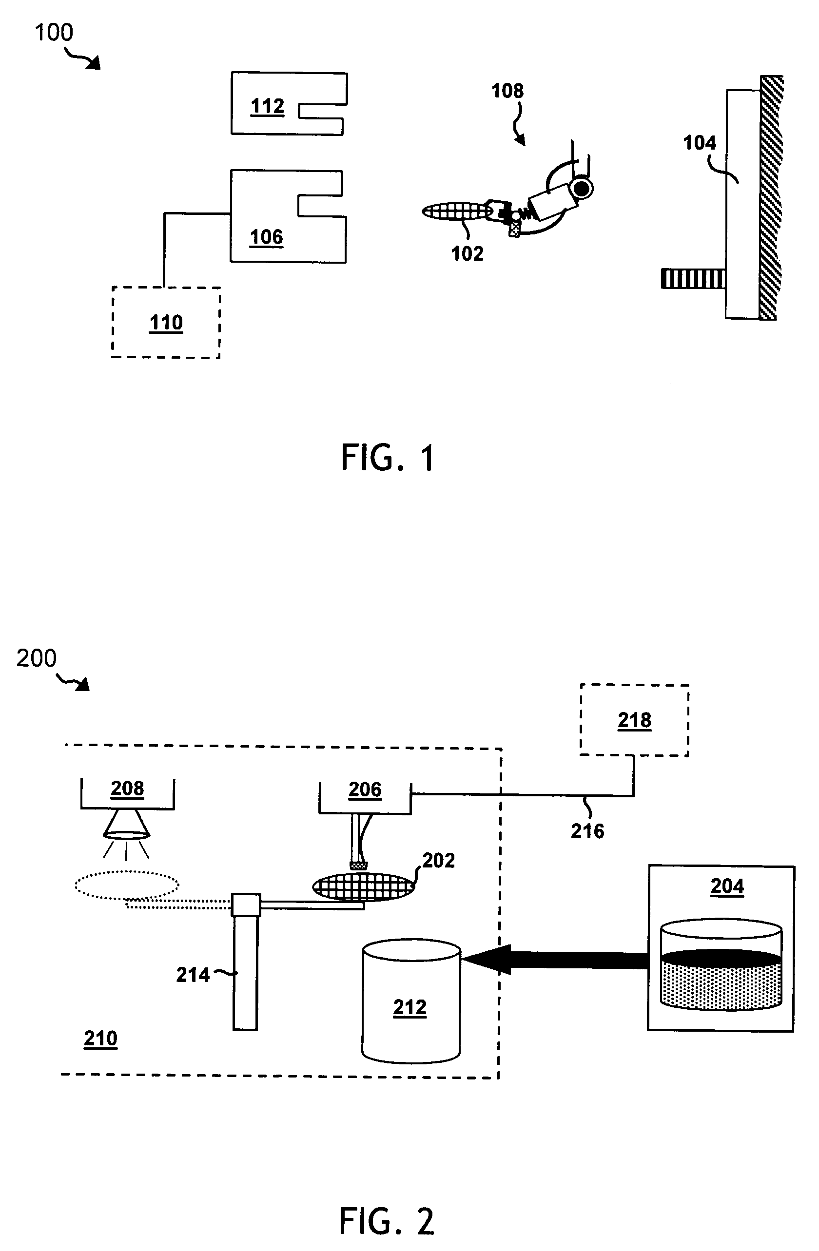
[0022]While the making and using of various embodiments of the present invention are discussed in detail below, it should be appreciated that the present invention provides many applicable inventive concepts, which can be embodied in a wide variety of specific contexts. The invention will now be described and illustrated in conjunction with a system for remediating copper cross-contamination occurring in a semiconductor manufacturing process. The specific embodiments discussed herein are, however, merely illustrative of specific ways to make and use the invention and do not limit the scope of the invention.

[0023]A remediation system according to the present invention operates in-line within a semiconductor manufacturing process. Time and labor are not lost transferring test wafers to a detection or inspection system. Instead, inspection of test wafers, or wafers suspected of having cross-contamination, is streamlined within the manufacturing or process flow. A remediation system acc...


PUM


Abstract

The present invention defines a system (100) for detecting copper contamination within a semiconductor manufacturing process. According to the present invention, a semiconductor wafer (102) is transferred (108) from a semiconductor manufacturing component (104), which may have exposed the wafer to copper contamination, to a measurement system (106). The measurement system measures an electrical value at a plurality of locations along a surface of the wafer, prior to and after exposure of the surface to an activation system (112). The activation system is provided to cause any copper contamination along the surface to form a precipitate thereon. An analysis component (110) is provided to receive electrical value and location information from the measurement system and to identify, from the measurements, the presence and location of copper contamination along the semiconductor wafer surface.

Description

TECHNICAL FIELD OF THE INVENTION[0001]The present invention relates generally to the field of semiconductor manufacturing processes and, more particularly, to apparatus and methods for detecting and remediating cross contamination in certain device fabrication processes.BACKGROUND OF THE INVENTION[0002]The continual demand for enhanced integrated circuit performance has resulted in, among other things, a dramatic reduction of semiconductor device geometries, and continual efforts to optimize the performance of every substructure within any semiconductor device. A number of improvements and innovations in fabrication processes, material composition, and layout of the active circuit levels of a semiconductor device have resulted in very high-density circuit designs. Increasingly dense circuit design has not only improved a number of performance characteristics, it has also increased the importance of, and attention to, semiconductor material properties and behaviors.[0003]The increase...

Claims


Application Information

Patent Timeline
Patent Type & Authority Patents(United States)
IPC IPC(8): G06F19/00G06K7/10H01L21/44H01L21/66
CPCH01L22/20Y10S438/935
Inventor RAMAPPA, DEEPAK A.
Owner TEXAS INSTR INC
Why Eureka
Try Eureka