System for ultraviolet atmospheric seed layer remediation

a seed layer and ultraviolet radiation technology, applied in the direction of cleaning process, semiconductor device details, semiconductor/solid-state device devices, etc., can solve the problems of copper being rather difficult to deposit directly on the dielectric via ecd, circuit generation generates numerous challenges to the semiconductor manufacturing process, and copper is very difficult to etch in most semiconductor process flows, etc., to achieve convenient, efficient and cost-effective

Inactive Publication Date: 2006-03-21
TEXAS INSTR INC
View PDF8 Cites 1 Cited by
  • Summary
  • Abstract
  • Description
  • Claims
  • Application Information

AI Technical Summary

Benefits of technology

[0012]The present invention provides a versatile system that neutralizes the effects of seed layer contamination and provides non-destructive seed layer remediation in an easy, efficient and cost-effective manner. The system of the present invention may be collocated, and even integrated, with other processing equipment (e.g., provided in situ within an ECD apparatus).
[0015]The present invention thus renders more hydrophilic seed layers—increasing effectiveness of the ECD plating process and resulting in higher yields and fewer reliability problems when compared to existing methods and systems.

Problems solved by technology

The increased packing density of the integrated circuit generates numerous challenges to the semiconductor manufacturing process.
Unfortunately, copper is very difficult to etch in most semiconductor process flows.
Unfortunately, however, copper tends to be rather difficult to deposit directly on dielectric via ECD, due largely to the material properties of copper and most common dielectric materials.
Obviously, this can cause a number of semiconductor yield and reliability problems.
Even though the seed layer approach eliminates some of the copper / dielectric interface problems, other complications arise from contamination of the seed layer.
Even if only exposed for a minimal time, the relative concentration of such contaminants on the seed layer surface can increase dramatically—causing any number of structural anomalies.
These anomalies in the seed layer surface can disrupt or inhibit the copper ECD process.
For example, certain anomalies can render the seed layer surface hydrophobic, causing voids and other unstable or incomplete copper device structures to form during a plating process.
Increased yield losses, device failures, and reliability problems result.
Isolation methods are effective for the period of time that a substrate is stored in isolation, but fail to address exposure and handling involved in transferring substrates into and out of storage.
Often, certain cleaning approaches are ineffective for particular contaminant chemistries.
Cleaning approaches can also further damage, or even remove, significant portions of the seed layer—rendering the seed layer unusable.
Seed repair methods often involve some measure of re-deposition of the seed layer—adding potentially numerous and costly extra processing steps.
Importantly, most all such approaches fail to eliminate the exposure of the seed layer surface to some contamination during transfer between the distinct processing apparatus involved.

Method used


Image

  • System for ultraviolet atmospheric seed layer remediation
  • System for ultraviolet atmospheric seed layer remediation

Examples


Embodiment Construction

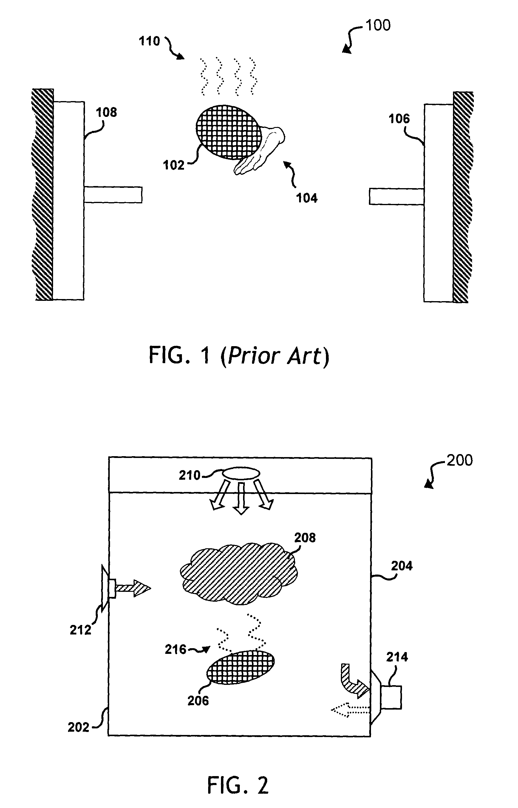
[0023]While the making and using of various embodiments of the present invention are discussed in detail below, it should be appreciated that the present invention provides many applicable inventive concepts, which can be embodied in a wide variety of specific contexts. The invention will now be described in conjunction with remediation of copper seed layers. The specific embodiments discussed herein are merely illustrative of specific ways to make and use the invention and do not limit the scope of the invention.

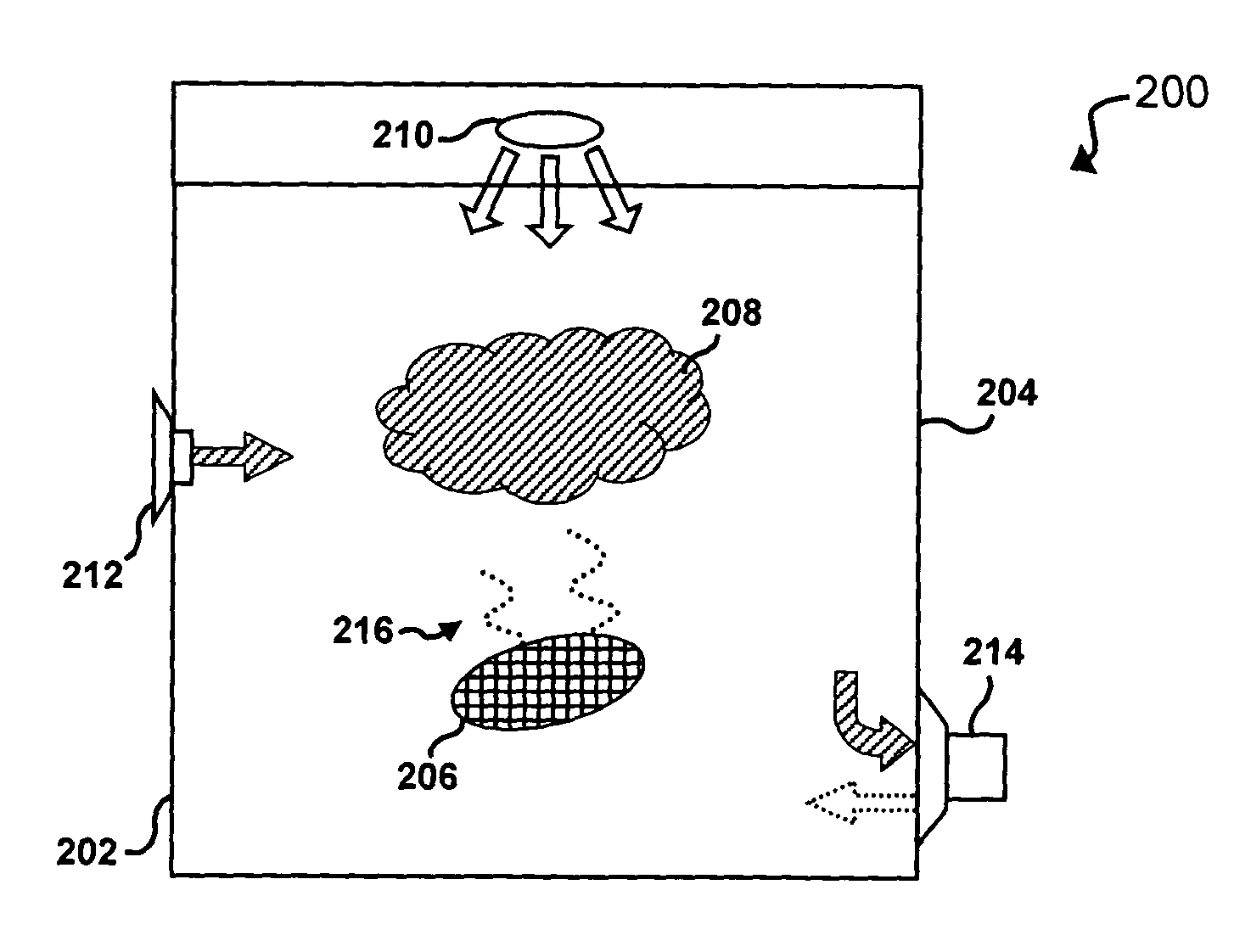
[0024]The present invention provides a system that remediates contaminants, and contaminant-based anomalies, from a seed layer surface in a non-destructive manner. The system of the present invention may be collocated, and even integrated, with other processing equipment (e.g., provided in situ within an ECD apparatus).

[0025]The present invention provides a remediation module. Handling systems or apparatus transfer a substrate, upon which a seed layer is already formed, int...


PUM

PropertyMeasurementUnit
densityaaaaaaaaaa
semiconductor material propertiesaaaaaaaaaa
packing densityaaaaaaaaaa

Abstract

The present invention provides a system for removing organic contaminants (216) from a copper seed layer that has been deposited on a semiconductor substrate (206). The present invention provides a housing (204) to enclose the semiconductor substrate within. An ultraviolet radiation source (210) is disposed within the housing. A treatment medium (208) is also provided within the housing. The semiconductor substrate is enclosed within the housing and exposed to the treatment medium. The ultraviolet radiation source exposes the semiconductor substrate to ultraviolet radiation, desorbing the contaminants from the seed layer.

Description

TECHNICAL FIELD OF THE INVENTION[0001]The present invention relates generally to the field of semiconductor devices and, more particularly, to apparatus and methods for remediating seed layer surfaces during device fabrication.BACKGROUND OF THE INVENTION[0002]The continual demand for enhanced integrated circuit performance has resulted in, among other things, a dramatic reduction of semiconductor device geometries, and continual efforts to optimize the performance of every substructure within any semiconductor device. A number of improvements and innovations in fabrication processes, material composition, and layout of the active circuit levels of a semiconductor device have resulted in very high-density circuit designs. Increasingly dense circuit design has not only improved a number of performance characteristics, it has also increased the importance of, and attention to, semiconductor material properties and behaviors.[0003]The increased packing density of the integrated circuit ...

Claims


Application Information

Patent Timeline
Patent Type & Authority Patents(United States)
IPC IPC(8): H01L23/552H01L21/28B08B7/00C25D5/34C25D7/12H01L21/00H01L21/288H01L21/304H01L21/321H01L21/768
CPCB08B7/0057H01L21/321H01L21/76873H01L21/76856H01L21/76862C25D5/34H01L21/67115H01L21/67028
Inventor FRANK, AARONGONZALEZ, DAVIDDEGENOVA, JOHNRAGHAVAN, SRINAVASRAMAPPA, DEEPAK A.
Owner TEXAS INSTR INC
Why Eureka
Try Eureka