
Method for driving an organic electroluminescent display device

a display device and electroluminescent technology, applied in the direction of electroluminescent light sources, static indicating devices, instruments, etc., can solve the problems of increasing luminance, lowering luminance, and small width of variations in luminance of organic electroluminescent elements with respect to current values, so as to reduce power consumption and suppress horizontal cross-talk or chrominance non-uniformity.

Inactive Publication Date: 2007-04-10
OPTREX CORP
View PDF6 Cites 4 Cited by
  • Summary
  • Abstract
  • Description
  • Claims
  • Application Information

AI Technical Summary

Benefits of technology

[0030]It is an object of the present invention to solve the problems stated earlier, to suppress the occurrence of horizontal cross-talk or chrominance non-uniformity in an organic electroluminescent display device and to reduce the power consumption required for the organic electroluminescent display device.
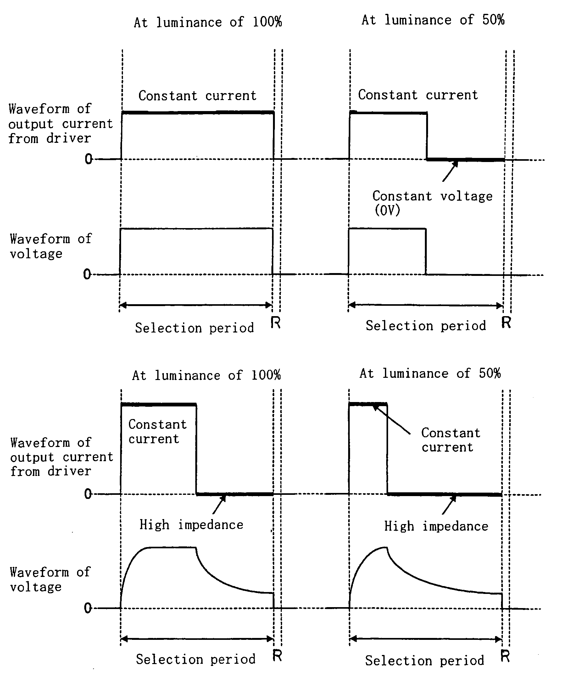
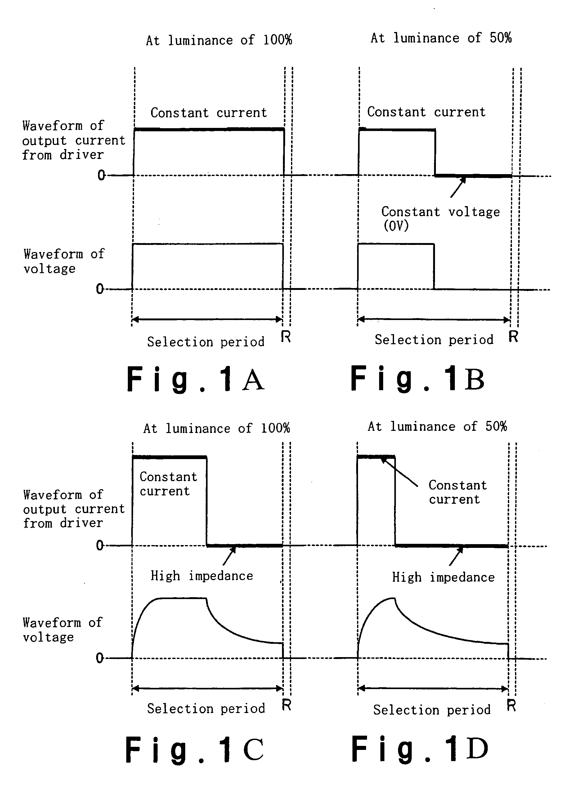
[0031]In order to attain the object, in a driving method according the present invention, special drive for capacitive charge, such as reset driving or precharge driving, is not performed, a driving section is set so as to have a shorter length than a selection period, and an amount of electric charges, which are supplied to pixels in the driving section in the selection period, is controlled so as to correspond to required luminance. In a driving method according the present invention, the electric charges that have been accumulated in the capacitance of the pixels in the driving period are controlled to be supplied to selected pixels in a non-driving period in the selection period. This form of driving method will be referred to as the electric charge control driving. When reset driving or precharge driving is not performed, an amount of currents that flow through the pixels is a period from start of drive to a time when an anode voltage has achieved a driving voltage is small, and the luminance is lower than an expected value in that period as stated earlier. However, it is possible to uniform the luminance amount in the selection period with respect to required luminance by controlling an amount of electric charges supplied to the pixels according to the required luminance. Thus, it is possible to reduce variations in luminance, and it is therefore possible to suppress the occurrence of horizontal cross-talk.
[0033]According to a second aspect of the present invention, there is provided a method comprising placing a data strip in a high impedance state after supplying a constant current to the data strip from the constant current circuit in the selection period for applying a selection voltage to a scanning strip, performing grayshade display by PWM, and supplying an amount of electric charges to the data strip in a constant current section when pixels emit light at respective gray scale levels, the amount of electric charges being calculated by adding an amount of residual electric charges to an amount of electric charges corresponding to luminance required for the respective gray scale levels, the amount of residual electric charges being found based on an estimated potential at the data strip at end of the high impedance section. In accordance with the second aspect, it is possible not only to obtain a desired luminance but also to suppress the occurrence of chrominance non-uniformity and horizontal cross-talk even in the case of a low gray scale level.
[0035]In the method according to a fourth aspect of the present invention, the organic electroluminescent element has luminous efficiencies to currents flowing therethrough falling in a variation range of 15% in a range of voltages applied across between an anode and a cathode of the organic electroluminescent element, the applied voltages ranging from the voltage applied at end of the rising time to the voltage applied at end of the high impedance section in the selection period in any one of the first to third aspects. In accordance with the fourth aspect, it is possible to obtain a uniform luminance even when the applied voltages greatly vary in the selection period.

Problems solved by technology

However, the width of variations in the luminance of an organic electroluminescent element is small with respect to the value of currents.
As a result, the pixels to emit light are short of electric charges, lowering the luminance.
As a result, the selected pixels have an excessive amount of electric charges, increasing the luminance.
However, in a case wherein the pixels have different current-voltage characteristics, the respective pixels have different values of currents flowing therethrough to fail to provide a uniform luminance over the entire screen even when the pixels have the same voltage applied thereacross.
As a result, there is caused chrominance non-uniformity wherein the luminance varies to portion from portion to such degree that can be visually recognized.
Even when a display pattern needs a small number of pixels to emit light, the power consumption for the organic electroluminescent display cannot be reduced to a lower value than the power consumption required for capacitive charge.

Method used


Image

  • Method for driving an organic electroluminescent display device
  • Method for driving an organic electroluminescent display device
  • Method for driving an organic electroluminescent display device

Examples


example 1

[0078]An organic electroluminescent element for passive matrix addressing was provided on a glass substrate. Specifically, an ITO film was deposited on the glass substrate so as to have a film thickness of 200 nm, and the deposited film was etched to form anode strips 2. A film of chrome (Cr) and a film of aluminum (Al) were deposited so as to have a layered structure having a film thickness of 300 nm, and the deposited layered structure was etched to form wiring in the organic electroluminescent element. On the etched structure, photosensitive polyimide was applied as an insulating film, and the applied film was exposed and developed to form openings working as light emitting portions of respective pixels. On the structure thus layered, a thin film was deposited to form a hole injection layer as an organic electroluminescent layer by a wet application method using an organic solvent containing PTPDEK as an organic polymeric material, PTPDEK is manufactured by Chemipro Kasei Kaisha,...

example 2

[0084]The organic electroluminescent element used in Example 1 was also used and energized at a frame frequency of 86 Hz and with a duty of 1 / 64 by the s electric charge control driving. The number of the gray scale levels was set at 16 (including a black level). As shown in Table 1, the driving current was 1.2 mA per one column. The current application section at the maximum gray scale level as the constant current section at the time of maximum luminance was set to have a length of 127 s. The current application section at the minimum gray scale except the black level was set to have a length of 5.8 μs. The impedance time at the maximum gray scale level was set at 49 μs, i.e., 70% of the selection time. The added pulse width was set at 5.4 μs.

[0085]The electric charge driving was performed by the conditions stated above. It was revealed that chrominance non-uniformity was not visually recognized and that no cross-talk was caused.


PUM


Abstract

In a selection period for applying a selection voltage to a scanning strip, a high impedance section for placing a data strip in a high impedance state is provided after a constant current section for supplying a constant current to a data strip from a constant current circuit. An organic electroluminescent element to be used has a small voltage-dependency in luminous efficiencies. When performing grayshade display by PWM, a data strip is supplied with an amount of electric charges from the constant current circuit in the constant current section, the amount of electric charges being calculated by adding an amount of residual electric charges in pixels to an amount of electric charges corresponding to luminance required for respective gray scale levels, the amount of residual electric charges being found based on an estimated potential at the data strip at end of the high impedance section.

Description

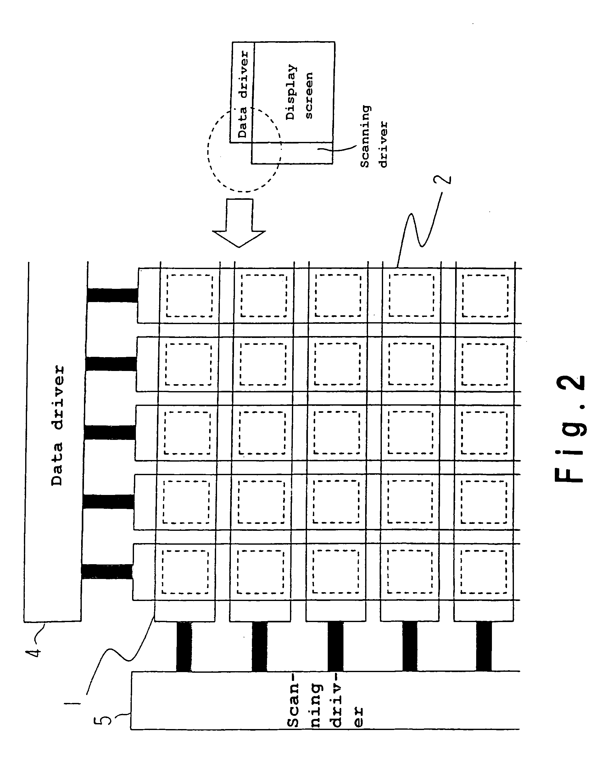
BACKGROUND OF THE INVENTION[0001]1. Field of the Invention[0002]The present invention relates to a method for driving an organic electroluminescent display device, which uses an organic electroluminescent light emitting element (hereinbelow, referred to as organic electroluminescent element).[0003]2. Discussion of Background[0004]An organic electroluminescent element has an organic thin film provided between an anode and a cathode. The organic thin film, which is sandwiched between both electrodes, has unnegligible capacitance formed therein. The organic electroluminescent element has properties similar to semiconductor light emitting diodes. When the anode side of the thin film is provided on a higher voltage side, and when a certain voltage is applied across both electrodes, the organic electroluminescent element emits light. Conversely, when the cathode side of the thin film is provided on a higher voltage side, the organic electroluminescent element does not emits light since al...

Claims


Application Information

Patent Timeline
IPC IPC(8): G09G3/30G09G3/32H01L51/50G09G3/20H05B33/00H05B33/14H05B33/22
CPCG09G3/3216G09G3/2014G09G2310/0251G09G2320/0209G09G2320/0223G09G2320/0233G09G2320/0252G09G2320/041
Inventor KATO, NAOKI
Owner OPTREX CORP
Learn More