
Method and apparatus for reducing capacitively coupled radio frequency energy between a semiconductor device and an adjacent metal structure

a capacitively coupled radio frequency energy and semiconductor technology, applied in cross-talk/noise/interference reduction, electrical apparatus construction details, printed circuit aspects, etc., can solve the problems of difficult to avoid metal structures close to semiconductor devices, electromagnetic interference, etc., to reduce the radiated emission, increase the distance between the source and the source, and maximize the absorption of radio frequency energy

Active Publication Date: 2007-04-17
ORACLE INT CORP
View PDF3 Cites 20 Cited by
  • Summary
  • Abstract
  • Description
  • Claims
  • Application Information

AI Technical Summary

Benefits of technology

"The patent describes a method and apparatus for reducing the amount of radio frequency energy emitted from a semiconductor device and absorbed by a nearby metal structure. This is achieved by using a bolster plate with a radio frequency energy absorptive material, such as a ferrite material, placed between the semiconductor device and the metal structure. The absorptive material is designed to absorb the specific frequency components of the radio frequency energy emitted by the semiconductor device. The method also involves detecting the range of radio frequency energy emitted, identifying a material that absorbs the energy, and securing the metal structure to the printed circuit board to reduce the source of interference. The technical effects of this invention include reducing interference between semiconductor devices and improving the performance of printed circuit boards."

Problems solved by technology

Any metal structure close to a packaged semiconductor device, such as a bolster plate used to secure the processor intermediate the printed circuit board (PCB) and a heat sink, absorbs the radio frequency (RF) energy at the various harmonic frequencies and becomes a source of electromagnetic interference (EMI).
Unfortunately, it is often difficult to avoid metal structures close to semiconductor devices because of thermal and mechanical constraints placed on printed circuit board design and the number semiconductor devices populated thereon.

Method used


Image

  • Method and apparatus for reducing capacitively coupled radio frequency energy between a semiconductor device and an adjacent metal structure
  • Method and apparatus for reducing capacitively coupled radio frequency energy between a semiconductor device and an adjacent metal structure
  • Method and apparatus for reducing capacitively coupled radio frequency energy between a semiconductor device and an adjacent metal structure

Examples


Embodiment Construction

[0023]References in the specification to “one embodiment” or “an embodiment” means that a particular feature, structure, or characteristic described in connection with the embodiment is included in at least one embodiment of the invention. The appearances of the phrase “in one embodiment” in various places in the specification are not necessarily all referring to the same embodiment.

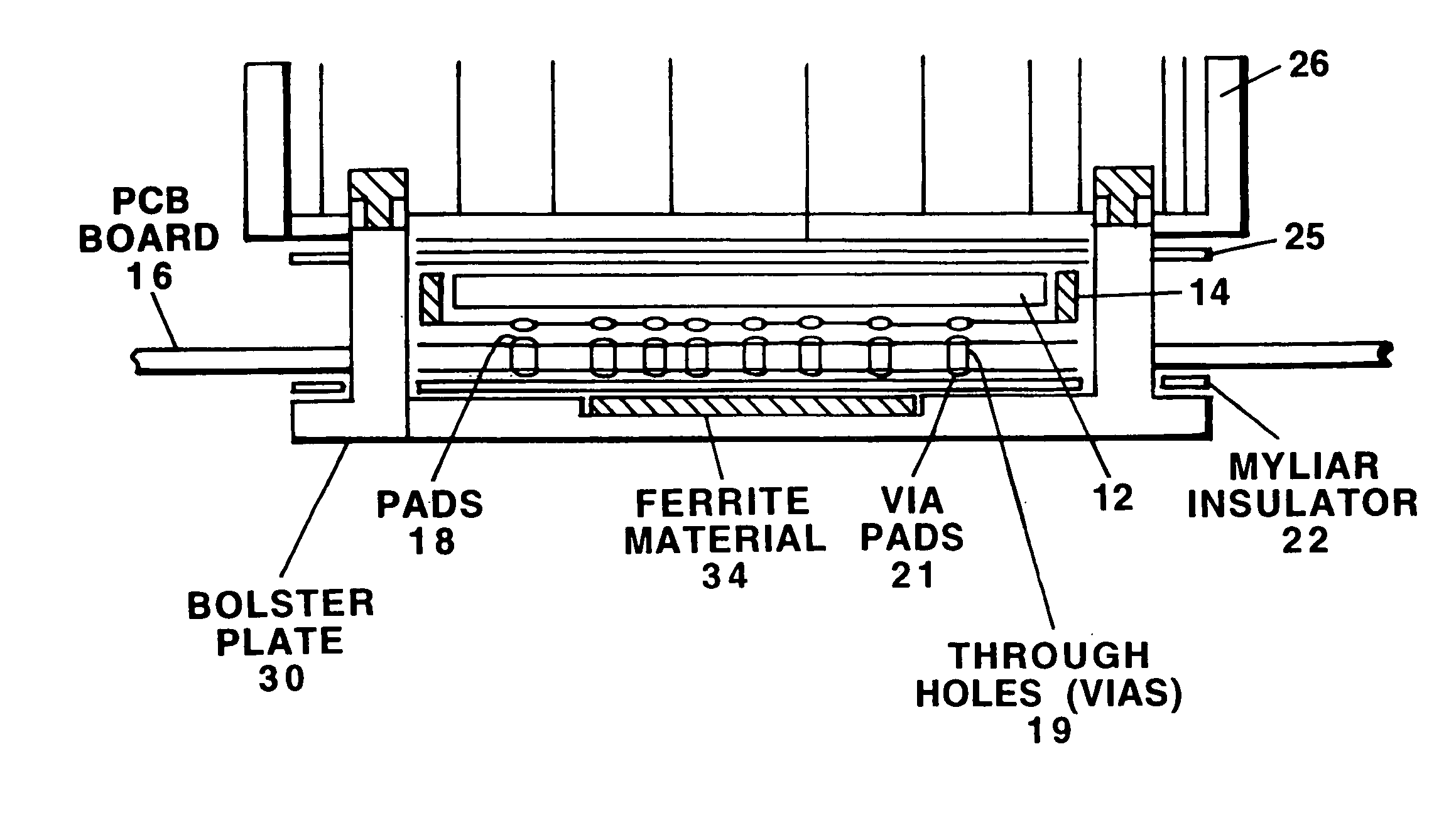
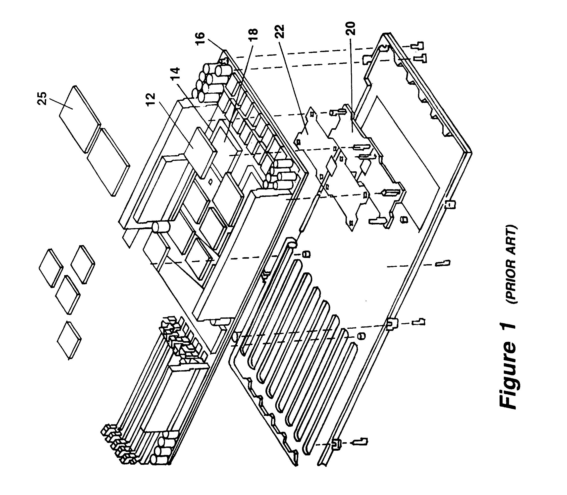
[0024]FIG. 1 is an exploded view of a prior art central processing unit (CPU) module assembly, such as the Ultrasparc III™ processor modules, commercially available from Sun Microsystems, Santa Clara, Calif., illustrating the relationship between semiconductor device(s) and the printed circuit board. As illustrated, the CPU processor 12 is surrounded by a socket 14 and is sits on top of pads 18 formed in the upper surface of PCB board 16. A bolster plate 20 is inserted from the underside of PCB board 16, through holes in Mylar sheet 22 and through holes PCB board 16. Mylar sheet 22 electrically isolates ...


PUM


Abstract

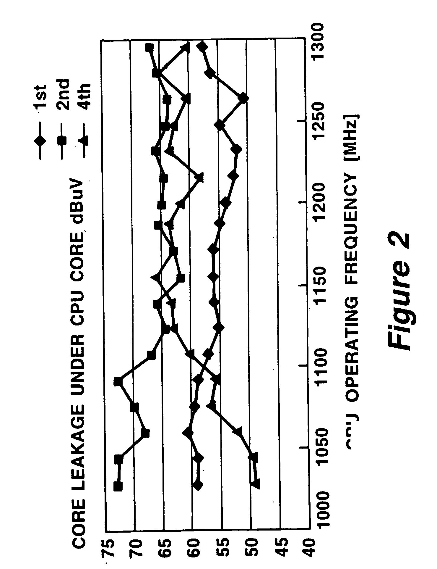
A bolster plate apparatus, used to secure a semiconductor device intermediate a printed circuit board and a heat sink apparatus, includes either an indentation or an open aperture into which a radio frequency absorptive material may be disposed. The absorptive material may be a ferrite material specifically selected to absorb frequencies in the range of the second to fourth harmonic of the processor clock signal frequency. The type of the ferrite material implanted in the bolster plate is selected to maximize the absorption of radio frequency energy, particularly that emitted at the pad vias on the underside of the printed circuit board, without affecting the signal integrity of the other pad connections. The shape of the cutout or aperture is also defined by the arrangement of RF emitting pads on the underside of the printed circuit board. The open aperture, without any absorptive material, effectively increases the distance between the source of the radio frequency energy and the metal body of the bolster plate, thereby reducing the amount of radio frequency energy absorbed by the bolster plate and the electromagnetic interference generated thereby. Also disclosed is a method for reducing the radiated emission from an adjacent semiconductor device by selectively removing pads from the undersurface of the PCB board to effectively reduce the sources of the radio frequency energy, and, therefore the amount of RF energy capacitively coupled with RF energy metal body of the bolster plate.

Description

FIELD OF THE INVENTION[0001]The present invention relates to the field of electromagnetic interference, and, more specifically, to a device for reducing the capacitively coupled radio frequency energy from semiconductor devices to adjacent metal structures.BACKGROUND OF THE INVENTION[0002]Packaged semiconductor devices, such as processors, utilize digital clocking to synchronize their interaction with other components in a computer the system. These clock signals have harmonic content, including second and fourth harmonics of the fundamental clock signal frequency, that is emitted when the clock signal is present. Any metal structure close to a packaged semiconductor device, such as a bolster plate used to secure the processor intermediate the printed circuit board (PCB) and a heat sink, absorbs the radio frequency (RF) energy at the various harmonic frequencies and becomes a source of electromagnetic interference (EMI). This effect is due to capacitive coupling of the radio frequen...

Claims


Application Information

Patent Timeline
Patent Type & Authority Patents(United States)
IPC IPC(8): H01R12/00H05K1/00
CPCH05K1/0233H05K3/0061H05K3/325H05K2201/086H05K2201/09745H05K2201/10719H05K2201/2009
Inventor BALASINGHAM, WIGNESWARAN W.NOVAK, ISTVANMOFFETT, ROBERT S.GONSALVES, DANIEL D.
Owner ORACLE INT CORP
Learn More