Cap for semiconductor device

a semiconductor device and cap technology, applied in the direction of semiconductor lasers, lasers, basic electric elements, etc., can solve the problems of high hemeticity and endurance, inability to give sufficient reliability for the semiconductor device cap, and inability to meet the requirements of high hemicity and endurance, etc., to achieve excellent hermeticity and humidity resistance, the effect of sufficient fixing strength

Active Publication Date: 2007-04-24
SHINKO ELECTRIC IND CO LTD
View PDF7 Cites 3 Cited by
  • Summary
  • Abstract
  • Description
  • Claims
  • Application Information

AI Technical Summary

Benefits of technology

[0011]An object of this invention is to provide a reliable cap for a semiconductor device which realizes containment of no lead in a manufacturing process using low-melting glass containing no lead as a fixing material for fixing a light transmissive member to a cap body and can give high hermeticity and humidity resistance required for a semiconductor laser device or an optical device.
[0018]The semiconductor device cap according to this invention realizes no containment of lead in a manufacturing process of the semiconductor device cap by fixing the light transmissive member to the cap body using leadless vanadate-series low-melting glass as the fixing material. Thus, it is provided as the cap for a semiconductor device which does not adversely affect the environment. Where the low-melting glass is molten to fix the light transmissive member to the cap body, the light transmissive member is fixed to the cap body through the eutectic alloy layer created by the eutectic reaction of vanadium (V) contained in the low-melting glass and the metal applied on the surface of the cap body, thereby providing the cap for a semiconductor device in which the light transmissive member is strongly fixed to the cap body and sufficient fixing strength and excellent hermeticity and humidity resistance are given.

Problems solved by technology

However, where the SnO—P2O5 series glass is used as the low-melting glass, as compared with the case of using Pb-series low-melting glass employed in the related art, the SnO—P2O5 series glass is problematic in hermeticiy and endurance.
This lead to a problem being incapable of giving sufficient reliability for the semiconductor device cap which requires high hemeticity and endurance.

Method used


Image

  • Cap for semiconductor device
  • Cap for semiconductor device
  • Cap for semiconductor device

Examples


embodiment 1

[0025

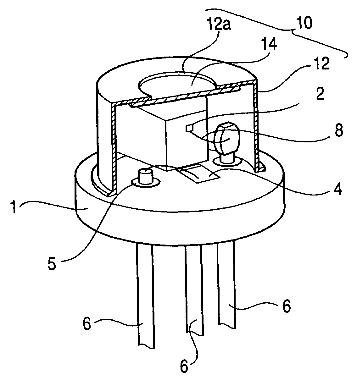
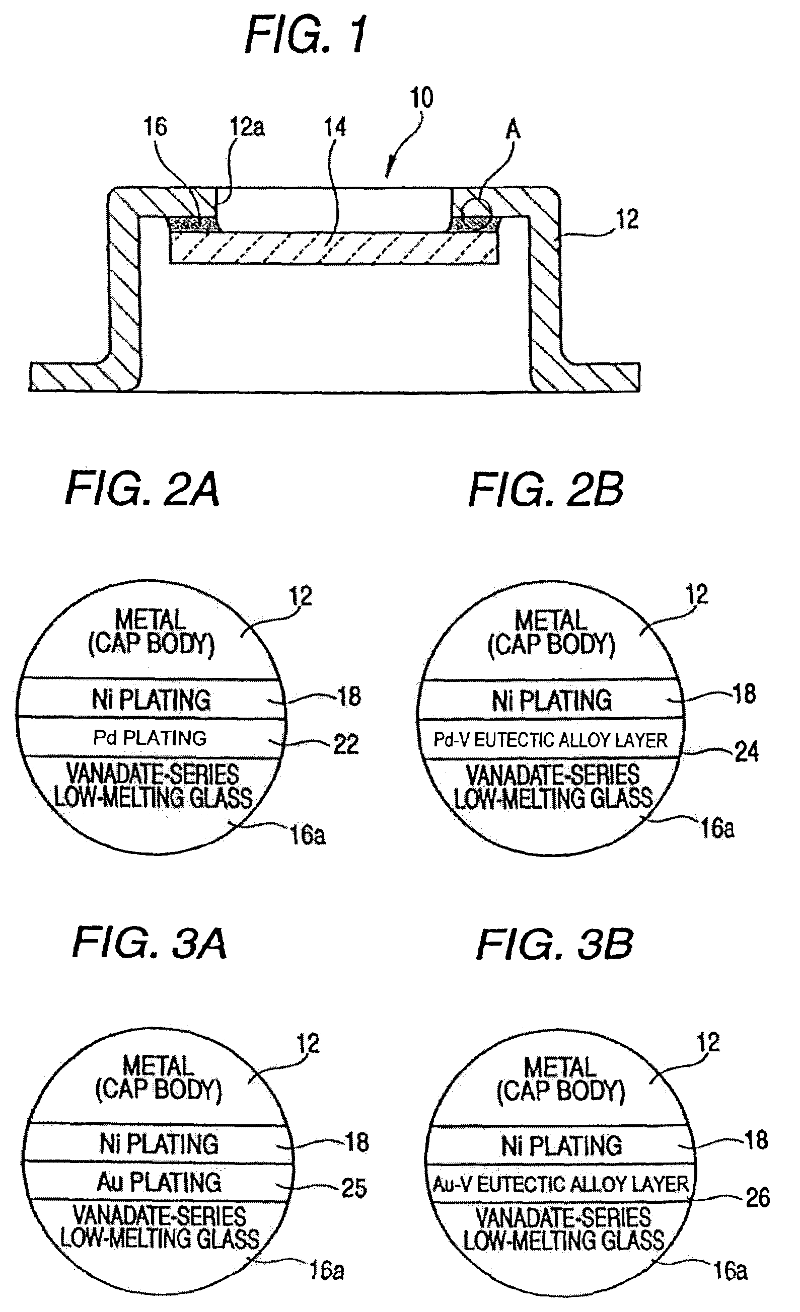
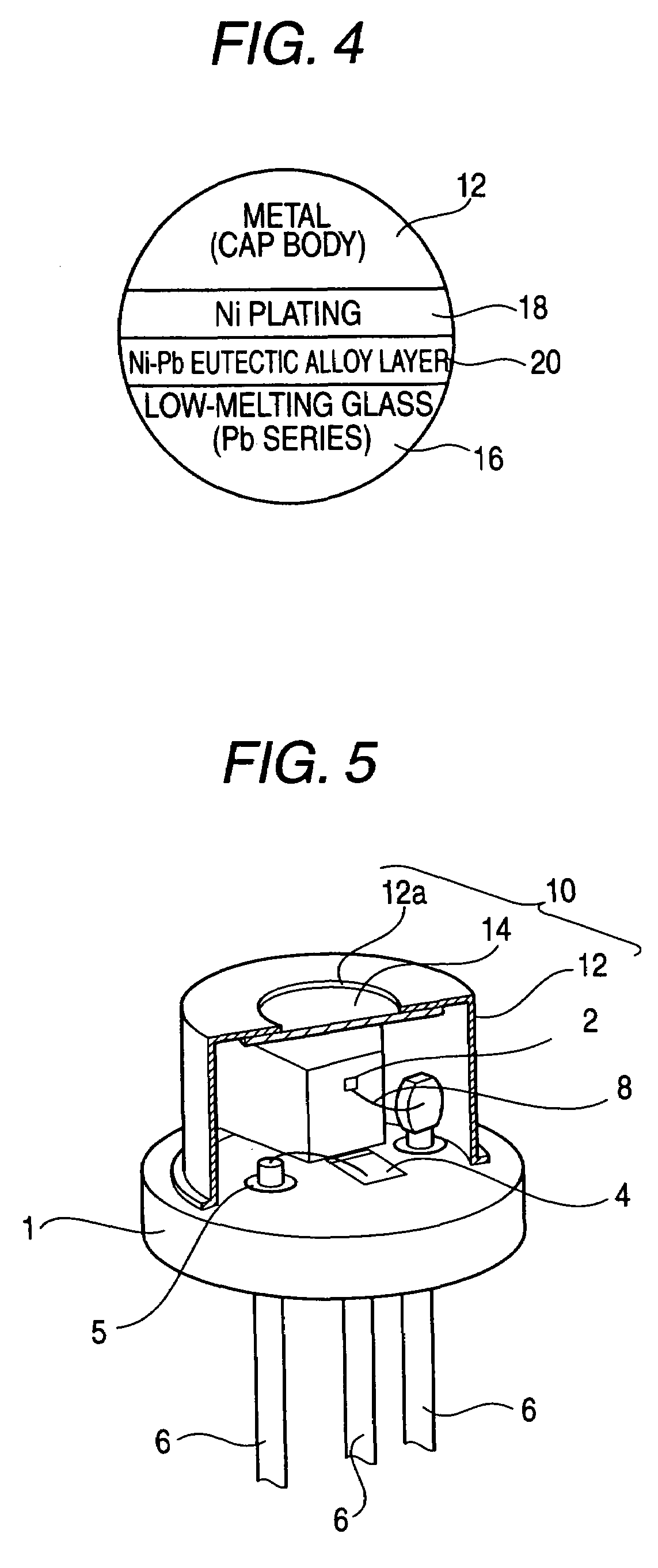
[0026]FIG. 1 is a sectional view showing the configuration of a semiconductor device cap 10 according to this invention. In this semiconductor device cap 10, a light transmissive window (light transmissive member) 14 is fixed to a cap body 12 using leadless low-melting glass 16 as a fixing material. The cap body 12 is formed in a cap shape having a flange at an opening edge by press-working a metallic material. At the upper part, a light transmissive opening 12a is formed. The light transmissive window 14 which is made of soft glass and disk-shaped is fixed to the edge of the light transmissive opening 12a so as to cover the light transmissive opening 12a by a low-melting glass 16 from the inside of the cap body 12. Incidentally, the material of the cap body 12 is not particularly limited, and may be e.g. iron, iron-nickel alloy, iron-cobalt-nickel alloy or alloy containing copper or nickel as a main component.

[0027]The features of the semiconductor device cap 10 according to t...

embodiment 2

[0050

[0051]As described above, where the vanadate-series low-melting glass is employed as the fixing material for fixing the light transmissive window 14 to the cap body 12, a gold plating, in place of the palladium plating, may be made on the surface of the cap body 12 so that through the eutectic alloy layer of gold and vanadium contained in the low-melting glass, the light transmissive window 14 can be fixed to the cap body 12. The semiconductor device cap according to the second embodiment is a semiconductor device cap manufactured through the gold plating made on the surface of the cap body 12.

[0052]FIG. 3 is an enlarged schematic view of the configuration (area A in FIG. 1) in the vicinity of the interface of the fixing area where the light transmissive window 14 is fixed to the cap body 12 with the gold plating 25 made on its surface using the vanadate series low-melting glass 16a. FIG. 3A shows the status before fixing and FIG. 3B shows the status after fixing.

[0053]The cap ...


PUM

PropertyMeasurementUnit
thicknessaaaaaaaaaa
thicknessaaaaaaaaaa
thicknessaaaaaaaaaa

Abstract

In a cap for a semiconductor device in which a light transmissive window is fixed to a cap body provided with a light transmissive opening using low-melting glass as a fixing material so that the light transmissive window covers the light transmissive opening, the low-melting glass is leadless vanadate-series low-melting glass, and the light transmissive window is fixed to the cap body through an eutectic alloy layer formed by an eutectic reaction of vanadium contained in the low-melting glass and metal applied on the surface of the cap body.

Description

BACKGROUND OF THE INVENTION[0001]1. Technical Field[0002]This invention relates to a cap for a semiconductor device, which is employed for assembling a semiconductor laser device used in e.g. an optical disk recording / reproducing apparatus, and more particularly to a cap for a semiconductor device in which light-transmissive member is fixed to a cap body using leadless low-melting glass.[0003]2. Related Art[0004]As a semiconductor laser device, the configuration as shown in FIG. 5 is known. This semiconductor laser device includes a disk-shaped metallic stem 1, a semiconductor laser element 2 serving as a light source, and a monitoring element 4 such as a PIN photodiode. The semiconductor laser element 2 is located on the side wall of a metallic block (heat sink) provided upright on the disk-shaped metallic stem 1. The monitoring element 4 is located below the semiconductor laser element 2 for monitoring the output from the semiconductor laser element 2. Lead pins 6 are passed throu...

Claims


Application Information

Patent Timeline
Patent Type & Authority Patents(United States)
IPC IPC(8): H01L29/22H01L33/00H01L23/02H01L23/10H01S5/022
CPCC03C3/062C03C3/122C03C8/24C03C27/044H01S5/02296H01L33/483H01L33/58H01S5/02212H01L2924/16151H01L2924/16152H01S5/02257H01S5/30
Inventor HATAKEYAMA, YASUSHI
Owner SHINKO ELECTRIC IND CO LTD
Why Eureka
Try Eureka