Ground bounce protection circuit for a test mode pin

Active Publication Date: 2007-05-01
XILINX INC
View PDF14 Cites 1 Cited by
  • Summary
  • Abstract
  • Description
  • Claims
  • Application Information

AI Technical Summary

Benefits of technology

[0012]A circuit is disclosed that allows the same pad to be used as a test pad for observing internal signals during test operations of an IC device and as an I/O pad during normal operation of the device while reducing the internal signals' susceptibility to undesirable fluctuations caused by switching events at the pad during normal operation. In accordance with the present invention, an IC device includes a reference circuit for generating a reference signal, a pad, and a test-mode circuit. The test-mode circuit, which is coupled between the pad and the reference circuit and is responsive to a control signal, is configured to selectively couple the pad and the reference circuit together during test operations and to isolate the pad and the reference circuit from each other during normal operations. For some embodiments, the control signal may be stored in a suitable storage element provided within the IC device. For one embodiment, level shifters may be used to level shift the control signal(s) provided to the test-mode circuit.
[0013]For some embodiments, the test-mode circuit includes first and second NMOS transistors and a PMOS transistor. The first NMOS transistor is coupled between the pad and a first node, and has a gate to receive the control signal. The PMOS transistor is coupled between the first node and a second node, and has a gate tied to ground potential. The second NMOS transistor is coupled between the second node and the reference circuit, and has a gate to receive the control signal. When the control signal is asserted (e.g.

Problems solved by technology

If the value of Vbg is not within an acceptable range or undesirably fluctuates during normal operation, the circuit may not operate properly.
Unfortunately, using the same pad as a test-mode pad for pre-packaging test operations and as an I/O pad for normal operations may render Vbg

Method used


Image

  • Ground bounce protection circuit for a test mode pin
  • Ground bounce protection circuit for a test mode pin
  • Ground bounce protection circuit for a test mode pin

Examples


Example

[0022]Like reference numerals refer to corresponding parts throughout the drawing figures.

DETAILED DESCRIPTION

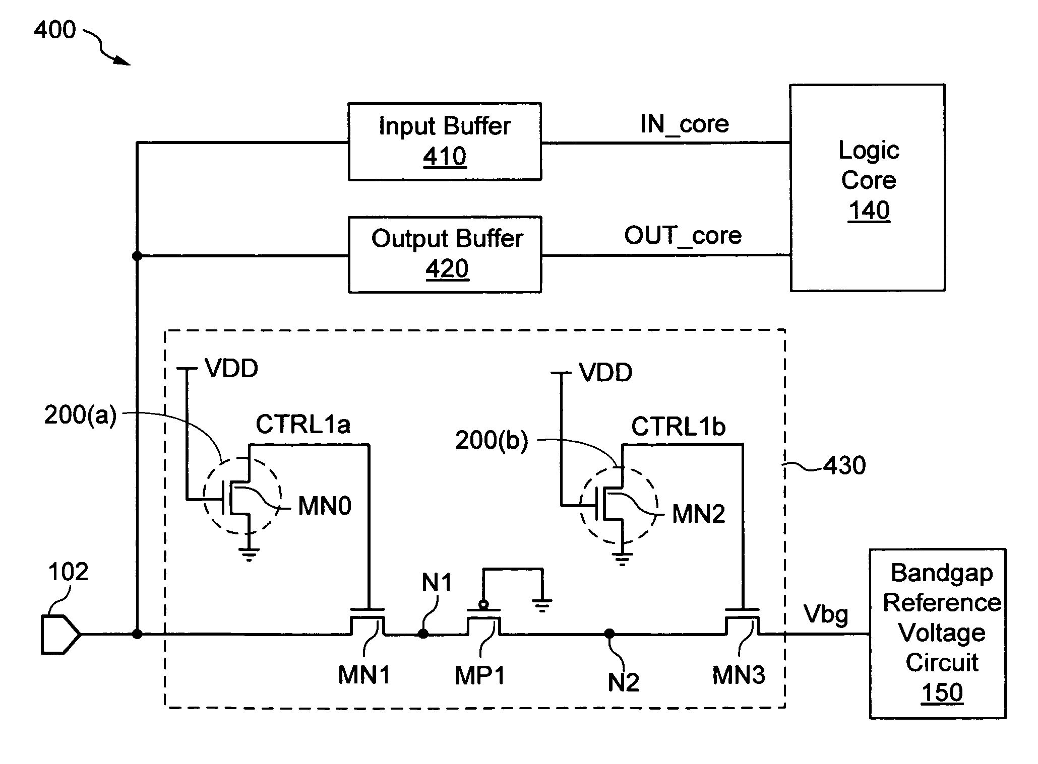
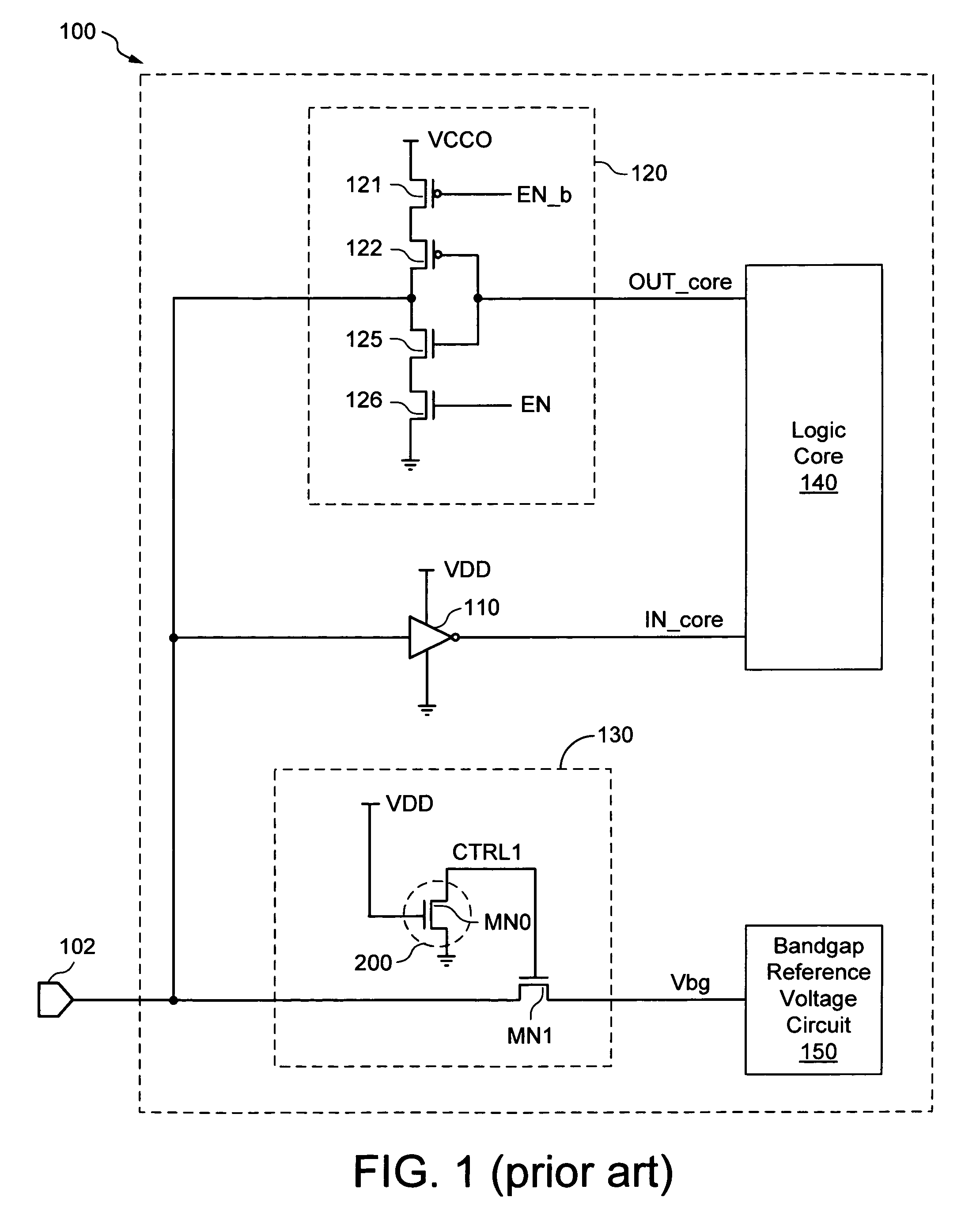
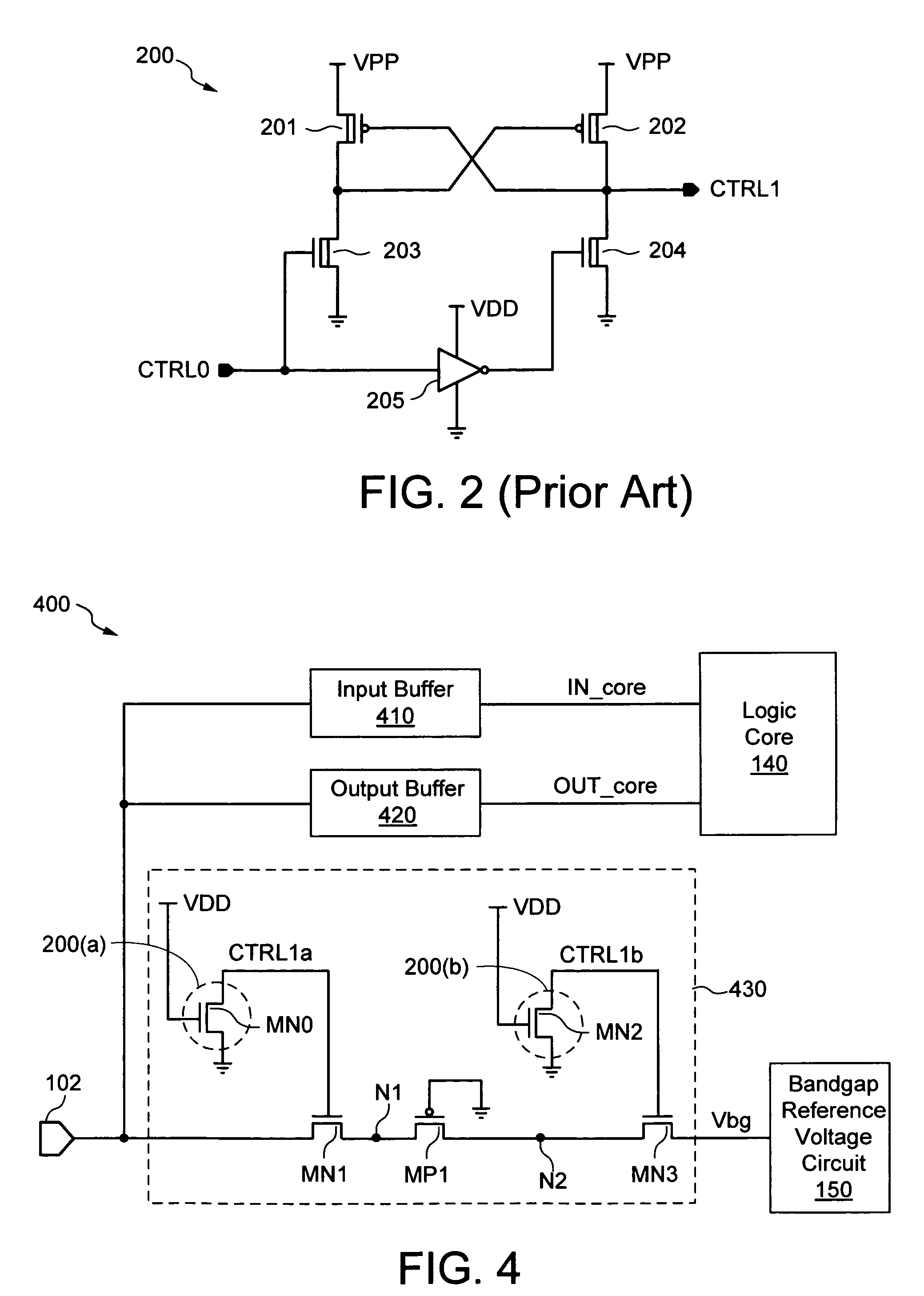
[0023]The present invention is applicable to a variety of integrated circuits and systems. The present invention has been found to be particularly applicable and beneficial for preventing ground bounce incurred during normal operation of an integrated circuit (IC) device from adversely affecting internal signals such as reference voltage signals generated within the IC device. In the following description, for purposes of explanation, specific nomenclature is set forth to provide a thorough understanding of the present invention. In other instances, well-known circuits and devices are shown in block diagram form to avoid obscuring the present invention. Further, the logic levels assigned to various signals in the description below are arbitrary, and thus can be modified (e.g., reversed polarity) as desired. Accordingly, the present invention is not to be construed as limited...


PUM


Abstract

A test-mode circuit allows the same pad of a semiconductor device to be used as a test pad during test operations and as an I/O pad during normal operations. The test-mode circuit is coupled between the pad and a reference signal (Vbg) of the device, and in response to a control signal (CTRL1) either couples the pad and the reference signal (Vbg) together or isolates the pad and the reference signal (Vbg) from each other. The test-mode circuit includes at least one NMOS transistor (MN1) and a PMOS transistor (MP1) connected in series between the pad and the reference signal (Vbg). During normal operation, the NMOS transistor (MN1) isolates the reference signal (Vbg) from the pad, and the PMOS transistor (MP1) compensates for voltage undershoot conditions at the pad.

Description

FIELD OF INVENTION[0001]The present invention relates generally to integrated circuits, and more specifically to reducing the susceptibility of a reference signal to undesirable fluctuations caused by switching events at an input / output pad of the circuit.DESCRIPTION OF RELATED ART[0002]A configurable integrated circuit (IC) is an integrated circuit including various configurable resources. A programmable logic device (PLD) is a well-known type of configurable IC that can be programmed by a user to implement a variety of selected functions. PLDs are becoming increasingly popular with circuit designers because they require less time to design than custom-designed integrated circuits such as Application Specific Integrated Circuits (ASICs).[0003]Many PLD's include one or more “test-mode” pads that allow test engineers to observe and test various important system signals internal to the PLD. For example, during pre-packaging test operations of a PLD, a test engineer may use the PLD's t...

Claims


Application Information

Patent Timeline
IPC IPC(8): H03K17/16
CPCG01R31/3004G01R31/31701H03K19/00315
Inventor ZHOU, SHI-DONGHUANG, GUBO
Owner XILINX INC
Why Eureka
Try Eureka