Drive circuit of TFTLCD

a technology of drive circuit and thin film transistor, which is applied in the direction of instruments, static indicating devices, etc., can solve the problems of large amount of devices, need of additional equipment to complete the connection between the drive circuit, and high wiring board cost, so as to increase the volume of the liquid crystal display, improve reliability, and reduce the cost

Active Publication Date: 2007-05-01
AU OPTRONICS CORP
View PDF15 Cites 14 Cited by
  • Summary
  • Abstract
  • Description
  • Claims
  • Application Information

AI Technical Summary

Benefits of technology

[0010]The invention provides a drive circuit, in which each source driver comprises a charge pump to compensate the voltage drop caused by the metal wire for power transmission. The large area flexible printed circuit board used in the prior art is not required, so that the increased volume of the liquid crystal display is obviated. In addition, the drive circuit provided by the invention has a simple fabrication process, such that the reliability is increased.

Problems solved by technology

The former method has the disadvantages including the usage of expensive wiring board (normally polyamide), requirement of large amount of devices, and the need of additional equipment to complete the connection between the drive circuit and the liquid crystal panel.
Moreover, when the terminal has a minute pitch, it further restricts the tape carrier pattern and the connection to the electrodes of the liquid crystal panel.
The resistance of the metal wires causes a significant voltage drop from one driver to the other.
The voltage drop seriously affects the normal operation of the drivers.
This method does not only increase the fabrication complexity of the flexible printed circuit board, but also increase the cost and the overall volume of the liquid crystal display.
Moreover, as the fabrication process is more complex, the reliability is decreased.

Method used


Image

  • Drive circuit of TFTLCD
  • Drive circuit of TFTLCD
  • Drive circuit of TFTLCD

Examples


Embodiment Construction

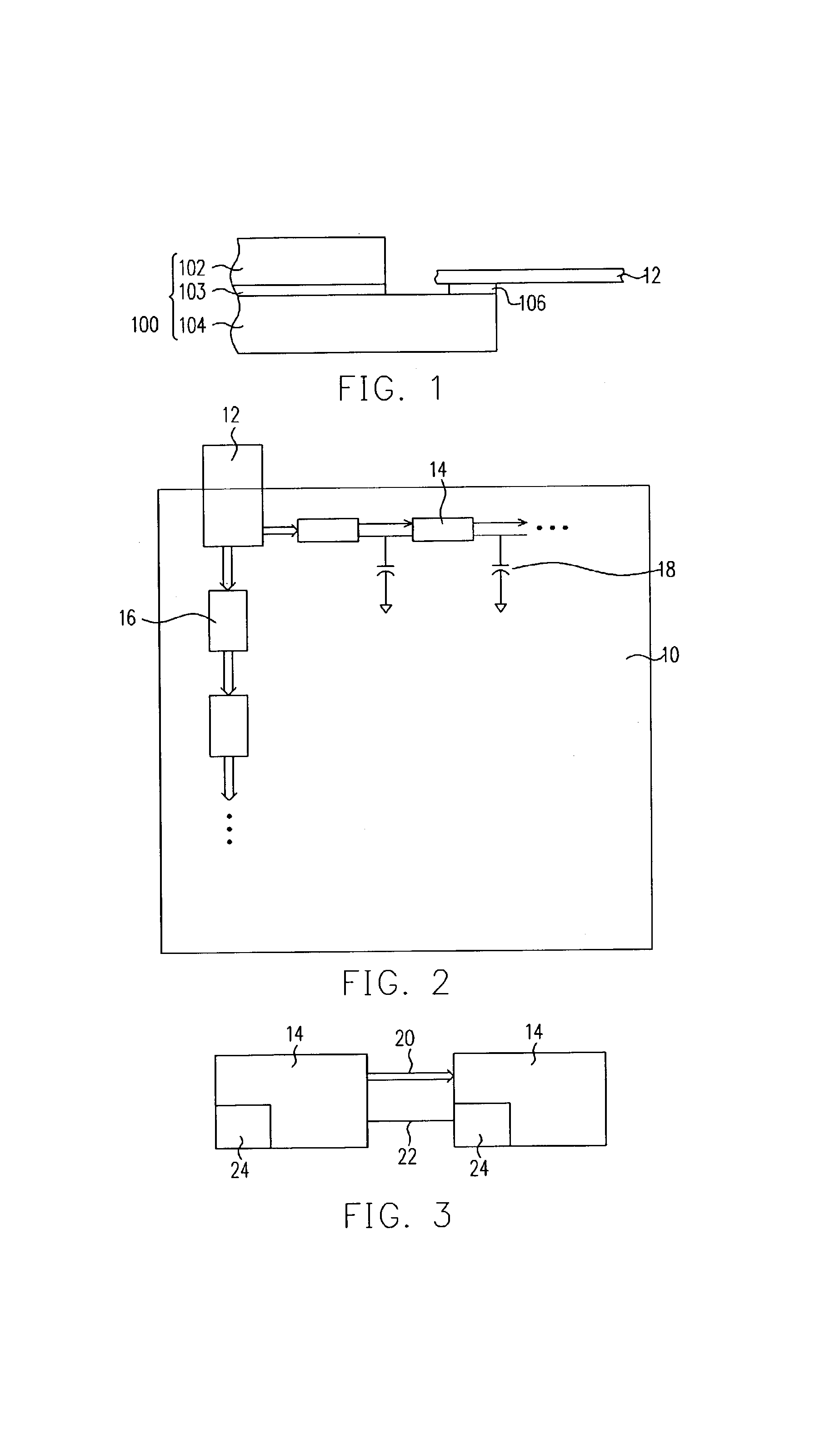
[0018]In FIG. 1, a typical chip on glass type liquid crystal display with multiple chips is shown. The liquid crystal display comprises a liquid crystal panel 100, a drive circuit (referred as 10 as shown in FIG. 2), and a flexible printed circuit board 12 to connect the liquid crystal panel and the drive circuit. The liquid crystal panel 100 further comprises a circuit array substrate, that is, the thin-film transistor substrate 104, a counter substrate 102 and a liquid crystal material filling the space between these two substrates 102 and 104. The connection between the flexible printed circuit board 12 and the liquid crystal panel 100 is typically achieved using an electrically anisotropic conductive thin film 106, for example.

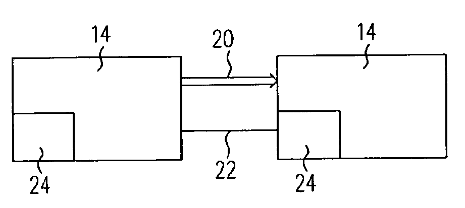
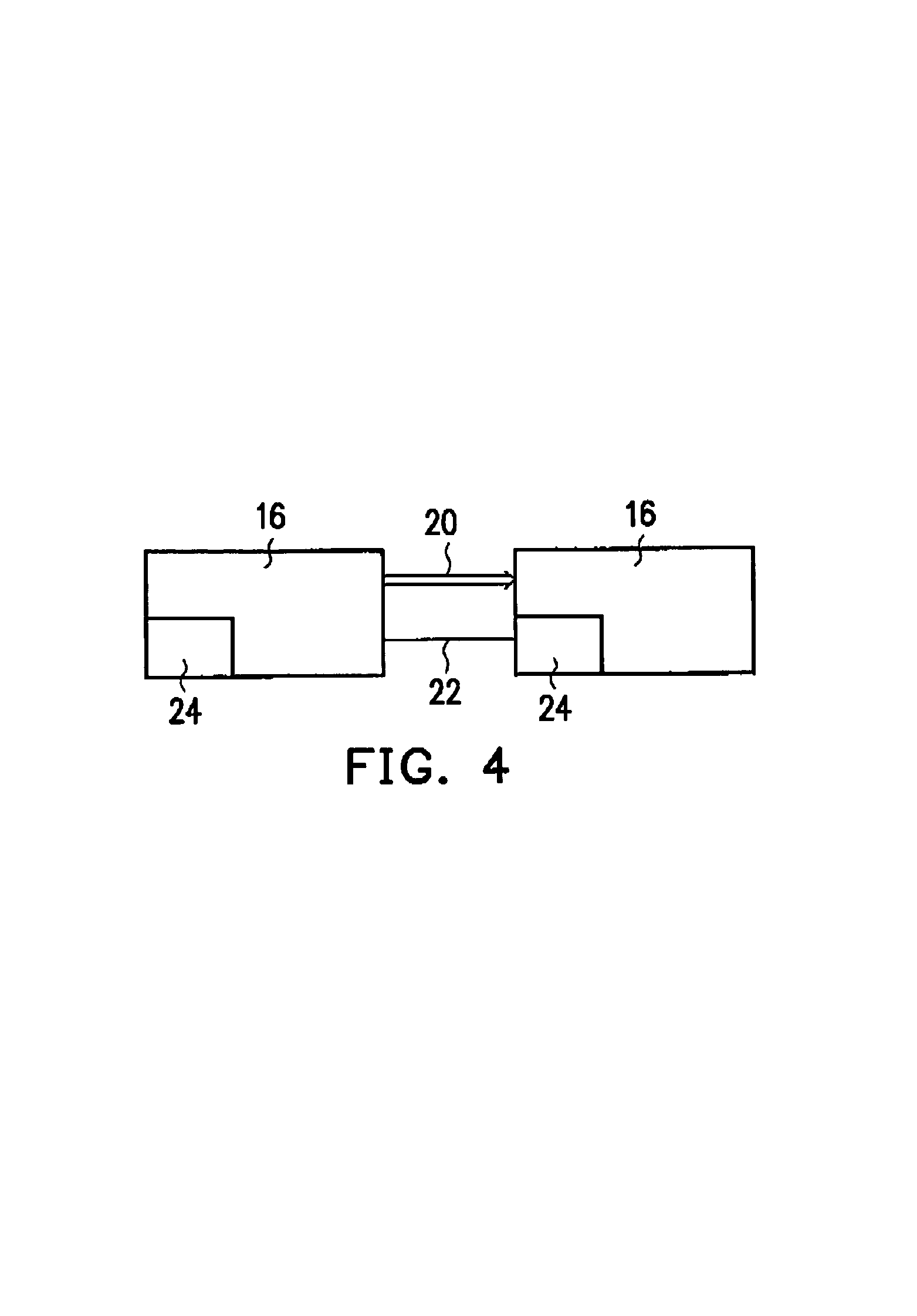
[0019]As mentioned above, in the conventional drive circuit, the power transmission between the source drivers are performed by the metal lines. Such metal lines have a resistance that generates a significant voltage drop, so that the drive circuit cannot ...


PUM


Abstract

A drive circuit of a thin-film transistor type liquid crystal display. A plurality of source drivers is connected in series. Each of the source drives has a charge pump therein to compensate the voltage drop caused by the metal wires for connecting the neighboring source drivers. The charge pump is preferably disposed at an input of the power line. A capacitor is further connected to each of the power lines for rectifying and filtering the power source transmitted by the power lines. The drive circuit also has a plurality of gate drivers. When the voltage drop caused by the power transmission line between the gate drivers is significant enough to affect a normal operation of the gate drivers, the charge pump is installed in each of the gate drivers.

Description

CROSS REFERENCE TO RELATED APPLICATIONS[0001]This application claims the priority benefit of Taiwan application serial no. 91112054, filed on Jun. 05, 2002.BACKGROUND OF INVENTION[0002]1. Field of the Invention[0003]The invention relates in general to a drive circuit of a thin-film transistor type liquid crystal display (TFTLCD), and more particularly, to a drive circuit that maintains a sufficient voltage to provide a normal operation of such drive circuit.[0004]2. Description of the Related Art[0005]Recently, the conventional widely used cathode ray tube (CRT) display has been gradually replaced by the flat panel display in small volume and light weight. Currently, the most popular flat panel display includes the liquid crystal display. The application of the liquid crystal display includes the low power products such as calculator, cellular phone, palm pilot, and the notebook computer, desktop computer, and even the wall television. To obtain an optimum display area of a liquid c...

Claims


Application Information

Patent Timeline
Patent Type & Authority Patents(United States)
IPC IPC(8): G09G3/36
CPCG09G3/36G09G2330/02
Inventor CHIANG, TSUNG-PEICHEN, CHUN-TA
Owner AU OPTRONICS CORP
Why Eureka
Try Eureka