Liquid crystal display apparatus having pixels with low leakage current

Inactive Publication Date: 2007-05-01
MITSUBISHI ELECTRIC CORP
View PDF15 Cites 32 Cited by
  • Summary
  • Abstract
  • Description
  • Claims
  • Application Information

AI Technical Summary

Benefits of technology

[0013]Accordingly, the primary advantage of the present invention is in suppression of an off-leakage current of a TFT element in a non-scanning period and reduction of voltage stress to a gate insulation film, which are achieved by serially connecting a plurality of TFT elements between a data line and a pixel electrode in each pixel, which can independently control the gate voltage.
[0014]As a result, display voltage retentivity in each pixel may be improved,

Problems solved by technology

Hence, the display voltage retentivity (data retentivity) in each pixel is significant, since lower display voltage retentivity requires a scan at higher frequencies, increasing the power consumption.
Therefore, the display voltage retentivity above may be degraded when the level of retained display voltage decreases due to a leakage current occurri

Method used


Image

  • Liquid crystal display apparatus having pixels with low leakage current
  • Liquid crystal display apparatus having pixels with low leakage current
  • Liquid crystal display apparatus having pixels with low leakage current

Examples


Example

[0028]First Embodiment

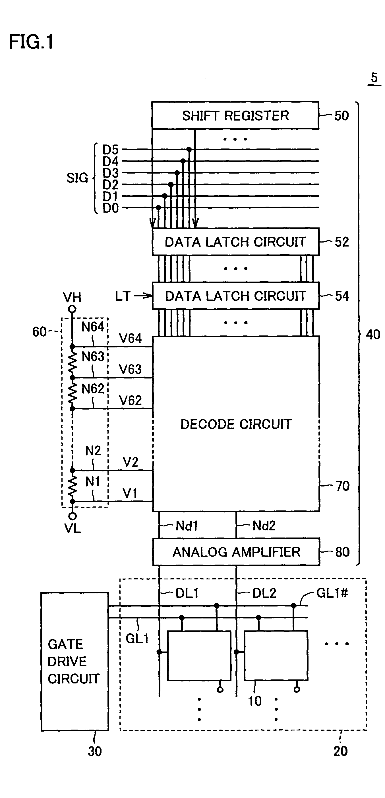
[0029]First, an overall configuration of a liquid crystal display apparatus according to an embodiment of the present invention is described.

[0030]Referring to FIG. 1, a liquid crystal display apparatus 5 includes a liquid crystal array portion 20, a gate drive circuit 30, and a source drive circuit 40. Liquid crystal array portion 20 includes a plurality of pixels 10 arranged in rows and columns. Corresponding to each row of pixels (hereinafter also referred to as “a pixel row”), a first gate line GL and a second gate line GL# are arranged. Further, corresponding to each column of pixels (hereinafter also referred to as “a pixel column”), a data line DL is arranged. FIG. 1 representatively shows pixels in the first and second columns in the first row, and corresponding gate lines GL1, GL1# and data lines DL1, DL2.

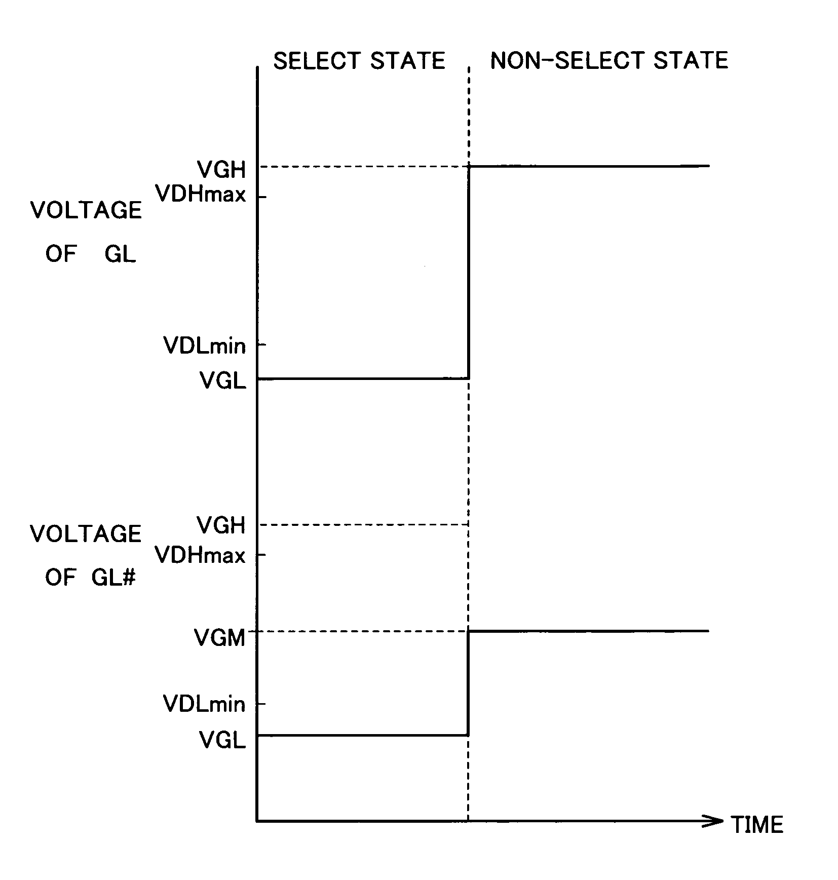
[0031]Gate drive circuit 30 controls the voltage of gate lines GL, GL# so that gate lines GL, GL# are set to a select state in a scanning period and ...

Example

[0097]Second Embodiment

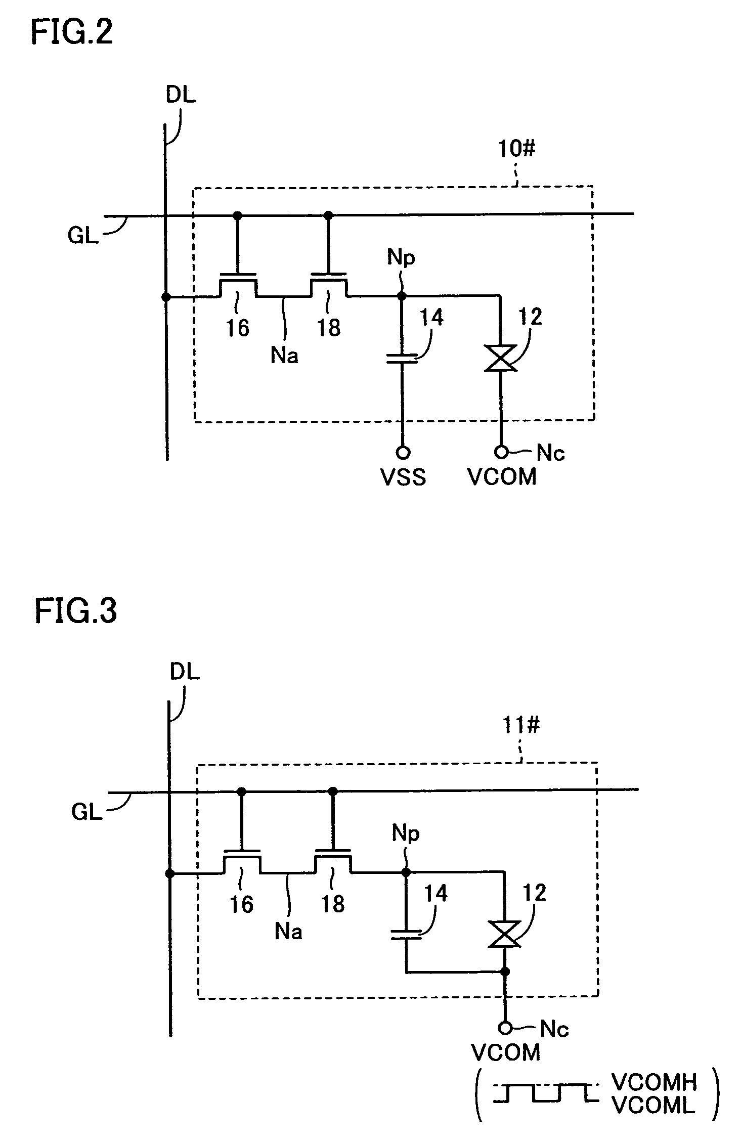
[0098]FIG. 7 is an equivalent circuit diagram showing a configuration example of a pixel according to a second embodiment.

[0099]A pixel 11 shown in FIG. 7 can be employed in place of pixel 10 in the overall configuration diagram of FIG. 1.

[0100]Referring to FIG. 7, pixel 11 according to the second embodiment is different from pixel 10 according to the first embodiment shown in FIG. 6 in that storage capacitor 14 is connected between pixel electrode node Np and a common electrode node Nc. Further, common voltage VCOM of common electrode node Nc is supplied as AC voltage with amplitude VD that is set alternately to low voltage VCOML and high voltage VCOMH in a constant cycle, as in pixel 11# in FIG. 3. Specifically, pixel 11 includes N-type TFT element 19 additionally to the components of pixel 11# of the comparative example shown in FIG. 3.

[0101]Similarly to pixel 10 shown in FIG. 4, each gate of N-type TFT elements 16, 18 is connected to gate line GL, while th...

Example

[0111]Third Embodiment

[0112]In the first and second embodiments, the configuration of a pixel is described in which a TFT element, of which gate voltage is set to intermediate voltage VGM in a non-select state, is provided in a leakage current path, to achieve both of leakage current suppression and protection of a gate insulation film of TFT element.

[0113]Though such a configuration is desirable for protecting a TFT element in a normal operation, it can not provide a desired stress to a TFT element in an acceleration test for screening defects in which a larger stress than in a normal operation is intentionally applied on the TFT element (a burn-in test). In the burn-in test, since the operation is tested under more severe condition than in a normal operation, i.e., in high temperatures and by applying a large voltage stress for a prescribed period, it is desirable to have a configuration that can provide sufficient voltage stress in a short time in order to perform the test effect...


PUM


Abstract

A pixel has first to third N-type TFT elements serially connected between a data line and a pixel electrode node. Each gate of the first and second TFT elements is connected to a first gate line, while the gate of the third TFT element is connected to a second gate line. The first and second gate lines in a select state each set to a high voltage that can fully turn-on the first to third TFT elements. The first gate line in a non-select state is set to a low voltage that can fully turn-off the first and second TFT elements, while the second gate line in the non-select state is set to an intermediate voltage between the maximum and the minimum voltages being transmitted on the data line.

Description

BACKGROUND OF THE INVENTION[0001]1. Field of the Invention[0002]The present invention relates to a liquid crystal display apparatus, and more specifically, to a liquid crystal display apparatus having a gate insulating field effect transistor in each pixel.[0003]2. Description of the Background Art[0004]As a display panel for a personal computer, a television receiver, a mobile phone, and a personal digital assistant, a liquid crystal display apparatus having liquid crystal elements as display pixels is used. Such a liquid crystal display apparatus is effective in reducing power consumption, size and weight, as compared to a conventional type.[0005]The display luminance of a liquid crystal element changes in accordance with the level of voltage applied thereon (hereinafter a voltage applied to a liquid crystal element is also referred to as “a display voltage”). The display panel of a liquid crystal display apparatus is formed with pixels each having a liquid crystal element. Each p...

Claims


Application Information

Patent Timeline
IPC IPC(8): G09G3/36G02F1/133G09G3/20G09G5/10
CPCG09G3/3659G09G2320/0214G09G2300/0814G09G2300/0809G02F1/133
Inventor TOBITA, YOUICHI
Owner MITSUBISHI ELECTRIC CORP
Why Eureka
Try Eureka