Optical waveguide device and optical waveguide module

a technology of optical waveguide and optical waveguide module, which is applied in the direction of optical waveguide light guide, instruments, optics, etc., can solve the problems of difficult to achieve large reduction effect, optical coupling loss, and the generation of matching error of mode profile, so as to reduce wavelength dependence and achieve low loss. , the effect of easy realization

Inactive Publication Date: 2007-05-01
NEC CORP
View PDF4 Cites 27 Cited by
  • Summary
  • Abstract
  • Description
  • Claims
  • Application Information

AI Technical Summary

Benefits of technology

[0017]An object of the present invention is to provide an optical waveguide device and an optical waveguide module which can easily realize low loss, reduction of wavelength dependence, and shape management in the manufacturing and testing processes.

Problems solved by technology

Therefore, matching error of mode profile is generated in the area immediately adjacent to the boundary.
Such matching error will cause an optical coupling loss.
However, such optical coupling loss may be reduced than that in the ordinary array waveguide grating illustrated in FIG. 1 but a problem rises here, in which it is difficult to attain large reduction effect.
As a result, a problem occurs here, that the scattering lights captured cannot be coupled within the waveguide array.
As a result, only the specific wavelength easily receives adverse effect.
Therefore, an additional problem occurs here, in which shape management of each waveguide path becomes difficult in the manufacture and testing.
As illustrated in FIGS. 3A to 3C, a similar problem is also generated in the low loss technique for star coupler and splitter of the related art.

Method used


Image

  • Optical waveguide device and optical waveguide module
  • Optical waveguide device and optical waveguide module
  • Optical waveguide device and optical waveguide module

Examples


Embodiment Construction

[0038]The exemplary embodiments of the present invention will be explained with reference to the accompanying drawings.

[0039]First, a structure of an array waveguide grating will be explained as a first exemplary embodiment of the present invention.

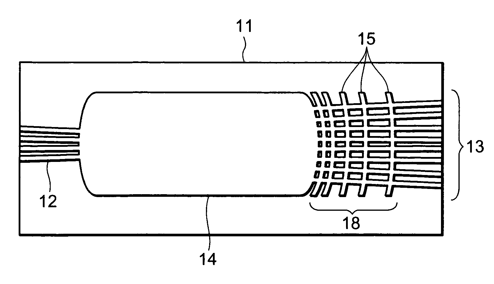
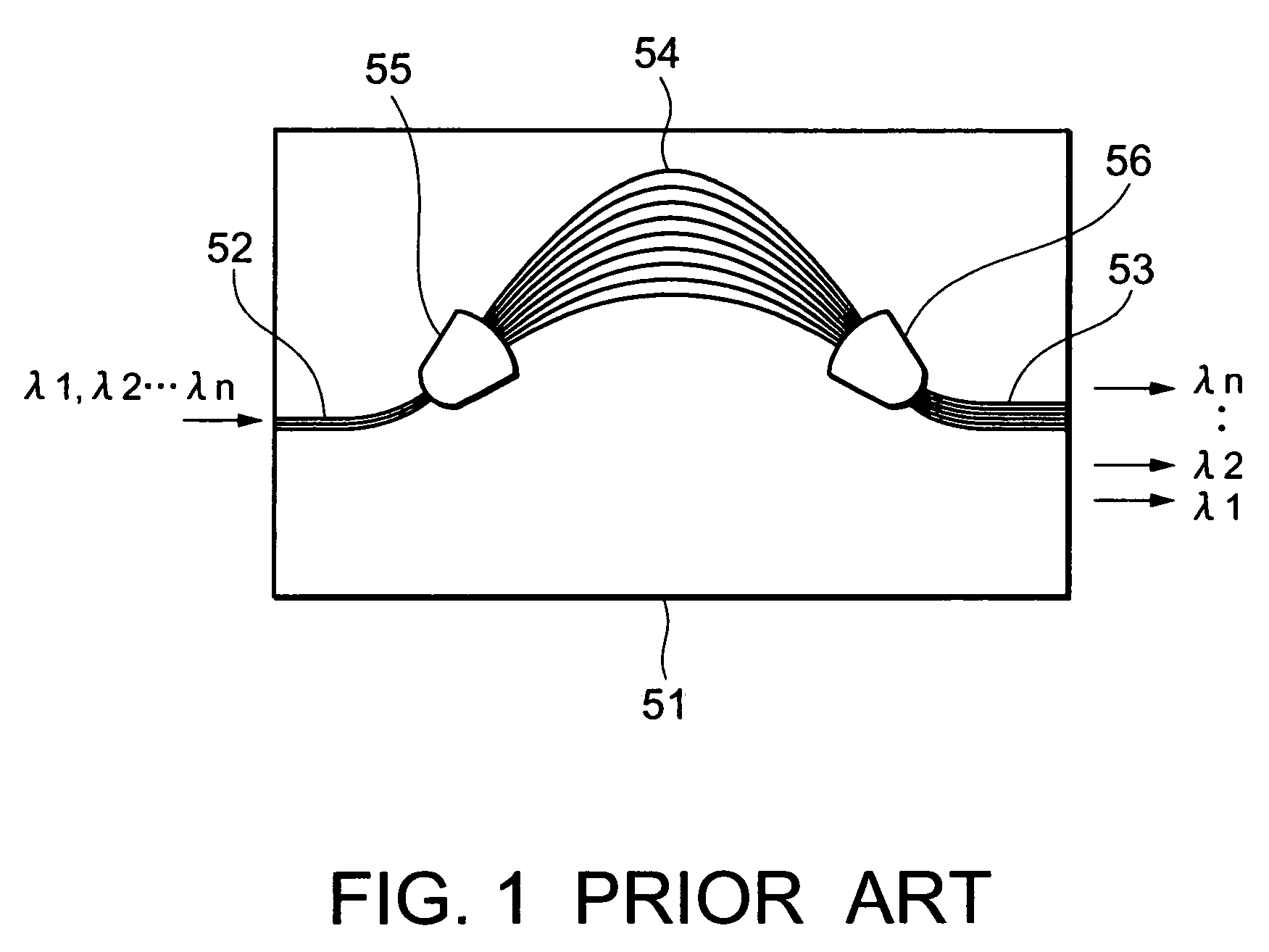
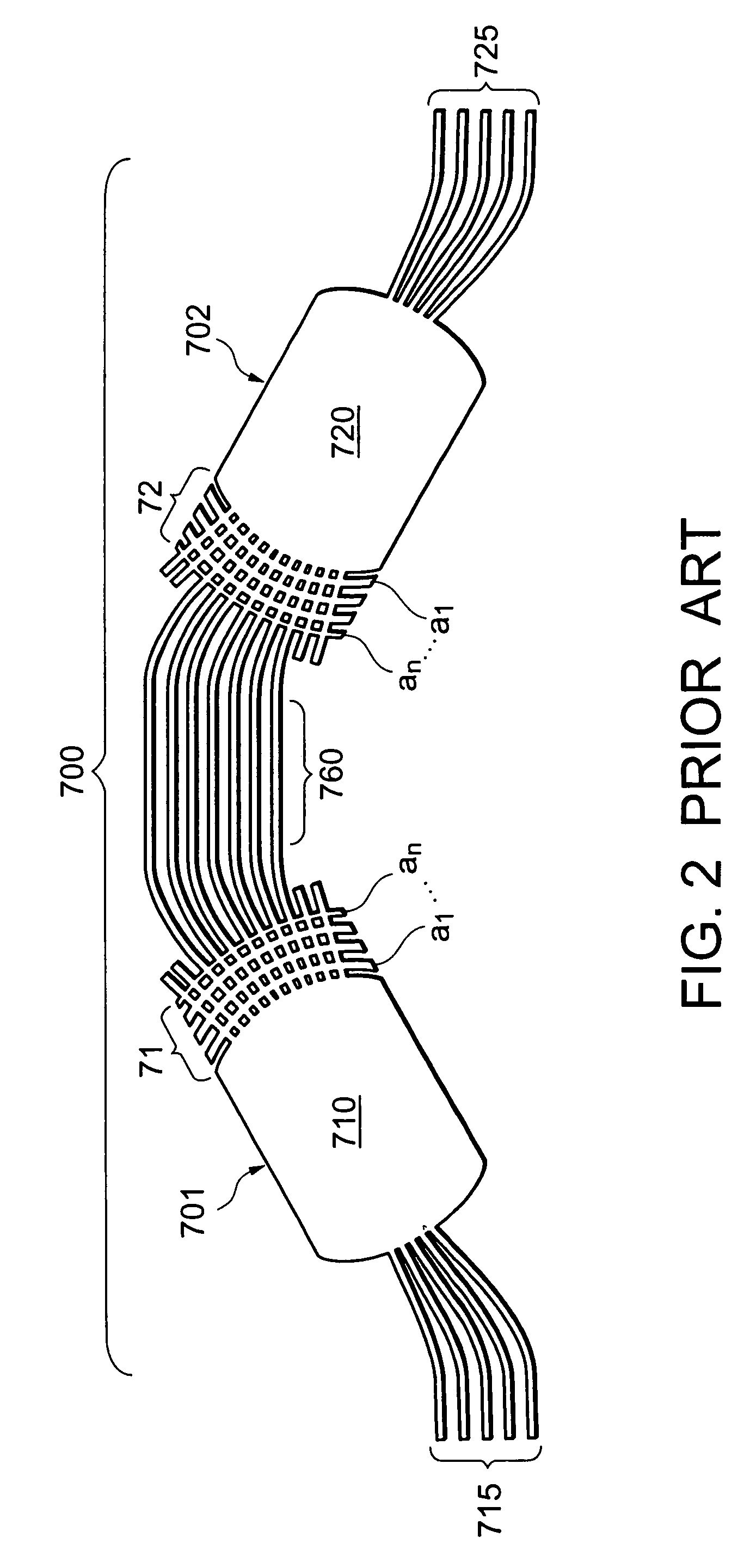
[0040]FIG. 5 is a plan view of the array waveguide grating of the first exemplary embodiment of the present invention, in which illustration (a) is a perspective view of the entire part, illustration (b) is a magnified diagram of the part A, and illustration (c) is a magnified diagram of the part B. The basic structure of this exemplary embodiment is constituted by forming, on a substrate 1, one or more input channel waveguides 2, a plurality of output channel waveguides 3, a channel waveguide array 4, a first slab waveguide 5 for connecting the input channel waveguides 2 and the channel waveguide array 4, and a second slab waveguide 6 for connecting the channel waveguide array 4 and the output channel waveguides 3. The channel waveguide ...


PUM


Abstract

An object of the present invention is to provide an optical waveguide device and an optical waveguide module having the function to multiplex / demultiplex or couple / decouple optical signals and particularly to provide an optical waveguide device and an optical waveguide module for realizing low optical loss, reducing wavelength dependence and ensuring easier shape management in the manufacturing and inspection processes. The optical waveguide device and optical waveguide module are provided with a substrate, one or more first waveguides, a plurality of second waveguides, and a slab waveguide for connecting the first waveguides and the second waveguides. At a region where the second waveguides are connected to the slab waveguide, a plurality of waveguide paths are provided for respectively connecting the second waveguides. Width of the waveguide paths is constant. The width of the separation gap between waveguide paths progressively increases as it becomes further away from the slab waveguide.

Description

BACKGROUND OF THE INVENTION[0001]1. Field of the Invention[0002]The present invention relates to an optical waveguide device used for optical communication and an optical waveguide module modified from the same optical waveguide device. Particularly, the present invention relates to an optical waveguide device and an optical waveguide module having the functions for multiplexing / demultiplexing or coupling / decoupling optical signals to reduce optical loss thereof.[0003]2. Description of Related Art[0004]In optical communication, further expansion of transmission capacity is expected. Accordingly, a wavelength division multiplexing optical transmitting method has widely been used because of its comparatively easier expandability in the transmission capacity. In recent years, further improvement in the degree of wavelength multiplexing is requested in the wavelength division multiplexing optical transmitting method. As a key device to realize such method, an optical multiplexing / demult...

Claims


Application Information

Patent Timeline
Patent Type & Authority Patents(United States)
IPC IPC(8): G02B6/34
CPCG02B6/12011G02B6/12014G02B2006/12147
Inventor HOSOI, TORU
Owner NEC CORP
Why Eureka
Try Eureka