Fin FET and method of fabricating same

a technology of fin fet and fin fet, which is applied in the direction of transistors, semiconductor devices, electrical equipment, etc., can solve the problems of increasing the junction leakage current, increasing the channel doping density, and increasing the wafer size, so as to improve the swing characteristics of the fin fet, improve the drain induced barrier lowering (dibl), and reduce the electric field of the channel and source/drain.

Active Publication Date: 2007-05-15
SAMSUNG ELECTRONICS CO LTD
View PDF7 Cites 41 Cited by
  • Summary
  • Abstract
  • Description
  • Claims
  • Application Information

AI Technical Summary

Benefits of technology

[0009]Exemplary embodiments of the invention provide a method of forming a fin field effect transistor (fin FET) by using a bulk silicon substrate, and a structure thereof. The fin FET is formed by forming a recess having a predetermined depth in a fin active region through use of the bulk silicon substrate, and then by forming a gate on an upper part of the recess, thereby guaranteeing a length of top channel formed under the gate. Also, lengths of top channel and bottom channel are uniformly formed in the fin active region by increasing a length of the top channel, thus improving swing characteristics of the fin FET. The top channel is formed lower than a source / drain region, thus improving a drain induced barrier lowering (DIBL) and reducing an electric field of channel and source / drain. The increase of top channel length can also reduce an impurity ion implantation amount of a threshold voltage control region formed under a gate, reducing a junction leakage current of the fin FET and improving refresh characteristics. In forming the recess having a predetermined depth in the fin active region there is no need to use a specific etch stop layer, thus simplifying a fabrication process of the fin FET. An upper edge portion of the fin active region is rounded, thereby preventing an electric field concentration onto an edge portion and a punch-through in the channel, and uniformly forming a gate insulation layer on an upper part of the fin active region.

Problems solved by technology

This causes a short channel effect, increases the channel doping density of transistors constituting a memory cell, and also increases the junction leakage current.
However, there are still some disadvantages that exist when the fin FET is formed on the SOI silicon substrate because the price of SOI wafers is higher than bulk wafers and the parasitic source / drain resistance increases.
Furthermore, a channel formation body of the semiconductor device is not connected to the SOI substrate according to a characteristic of the SOI device, thus a floating body effect is present, and heat generated in the device that is typically conducted to the SOI silicon substrate is cut off by an oxide layer formed on the SOI silicon substrate, thus degrading the performance of the semiconductor device.

Method used


Image

  • Fin FET and method of fabricating same
  • Fin FET and method of fabricating same
  • Fin FET and method of fabricating same

Examples


Embodiment Construction

[0014]Exemplary embodiments of the invention are more fully described in detail with reference to the accompanied drawings. The invention may be embodied in many different forms and should not be construed as being limited to the exemplary embodiments set forth herein. Rather, these exemplary embodiments are provided so that this disclosure is thorough and complete, and to convey the concepts of the invention to those skilled in the art.

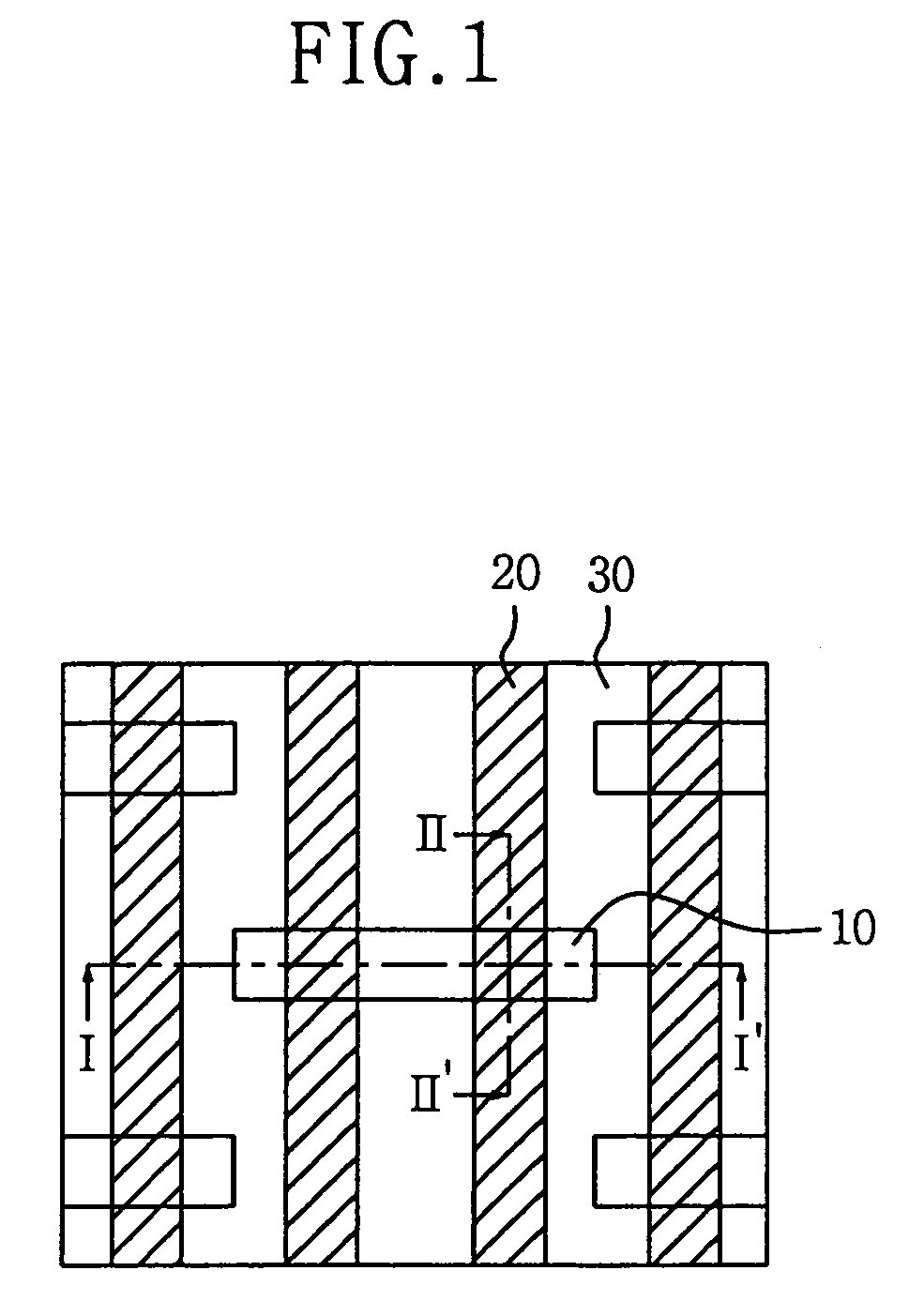
[0015]FIG. 1 is a layout diagram illustrating a fin FET according to some embodiments of the invention.

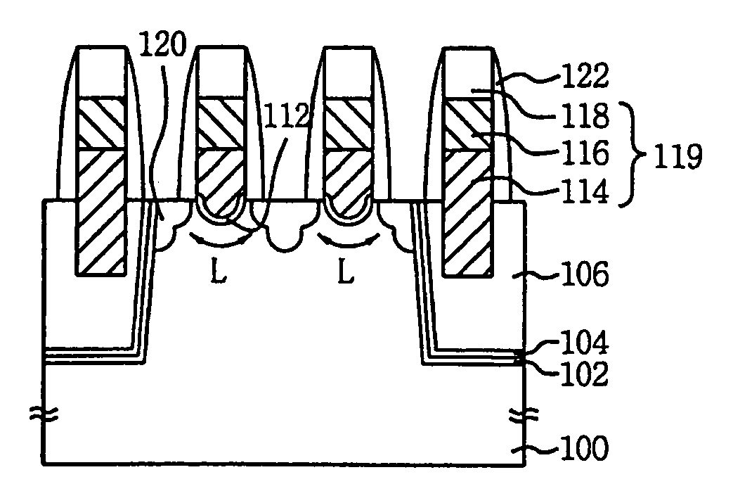
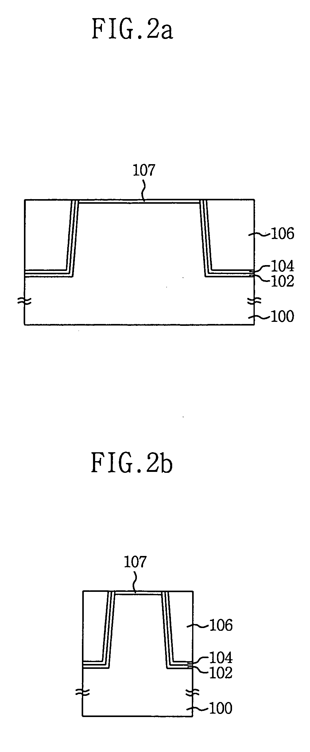
[0016]Referring to FIG. 1, gate electrodes 20 are patterned and disposed in parallel with one another along lines that extend in a first direction, for example, the line II–II′. Fin active regions 10 are disposed along parallel lines that extend in a second direction, for example, the line I–I′. The second direction is substantially perpendicular to the first direction. The fin active regions 10 are not continuous along the parallel lines that exten...


PUM


Abstract

A fin field effect transistor (fin FET) is formed using a bulk silicon substrate and sufficiently guarantees a top channel length formed under a gate, by forming a recess having a predetermined depth in a fin active region and then by forming the gate in an upper part of the recess. A device isolation film is formed to define a non-active region and a fin active region in a predetermined region of the substrate. In a portion of the device isolation film a first recess is formed, and in a portion of the fin active region a second recess having a depth shallower than the first recess is formed. A gate insulation layer is formed within the second recess, and a gate is formed in an upper part of the second recess. A source / drain region is formed in the fin active region of both sides of a gate electrode.

Description

CROSS REFERENCE TO RELATED APPLICATIONS[0001]This application claims priority from Korean Patent Application No. 2004-7426, filed on 5 Feb. 2004, the content of which is hereby incorporated by reference in its entirety for all purposes.BACKGROUND OF THE INVENTION[0002]1. Field of the Invention[0003]This disclosure relates to a semiconductor memory device, and more particularly, to a fin field effect transistor where a fin type active region is formed.[0004]2. Description of the Related Art[0005]Recently continuous requirements for semiconductor memory devices having lower power consumption, higher efficiency, and improved speed operation characteristics have brought about a continuously reduced design rule for the purposes of integrating more semiconductor memory devices within a semiconductor chip of a limited size. However, as semiconductor memory devices become increasingly integrated, the channel length of individual devices is gradually reduced. This causes a short channel effe...

Claims


Application Information

Patent Timeline
Patent Type & Authority Patents(United States)
IPC IPC(8): H01L21/336H01L29/76H01L29/786
CPCH01L29/66621H01L29/7854H01L29/66795H01L29/0657H01L29/7851H01L29/7856H01L21/18H01L21/823412H01L21/823431H01L21/823481H01L27/0886H01L29/0653H01L29/4236
Inventor KIM, KEUN-NAMYANG, HUNG-MOLEE, CHOONG-HO
Owner SAMSUNG ELECTRONICS CO LTD
Why Eureka
Try Eureka